
Einleitung
Ich habe mir gedacht, dass eine separate Übersicht über die verfügbaren DDR1 Ram Chips, ihr Verhalten bei Übertaktung und das -potenzial sicher einigen hier im Forum weiterhilft. Außerdem möchte ich Detailsaufnahmen der Chips zusammenstellen, damit man umgelabelte Chips einfacher identifizieren kann. Außerdem können wir noch einfache Tests dazunehmen, mit denen man die jeweiligen Chip erkennen kann, falls sie z.B. unter Heatspreadern verborgen sind. Das Ganze soll nach Hersteller und Chiptyp sowie -kapazität sortiert sein.
Kurzlinks zu den jeweiligen Herstellern:
Aeneon / Infineon / Qimonda | Elpida | Hynix | Micron | Mosel Vitelic | Nanya / Elixir | Promos | Samsung | Winbond |
Umgelabelte Chips
Usertests
SPD Tool

 www.hardwareluxx.de
SPDTool Tutorial
SPD Inhalt entschlüsselt:
inf
Aeneon/Infineon/Qimonda
Bezeichnung von Infineon Chips:
elp
Elpida
hyn
Hynix
Bezeichnung von Hynix Chips:
mic
Micron
Bezeichnung von Micron Chips:


Quellen:
256mb: https://www.micron.com/-/media/client/global/documents/products/data-sheet/dram/ddr1/256mb_ddr.pdf
512mb: https://www.micron.com/-/media/client/global/documents/products/data-sheet/dram/ddr1/512mb_ddr.pdf
1gb: https://www.micron.com/-/media/client/global/documents/products/data-sheet/dram/ddr1/1gb_ddr.pdf
mov
Mosel Vitelic
nan
Nanya / Elixir
Chip Bezeichnung
pro
Promos
Chip Bezeichnung

sam
Samsung
Bezeichnung von Samsung Chips:


win
Winbond
usertests
Usertests
----
Stand:
#630 (inkl. umgelabelte Chips)
#1050 (ohne umgelabelte Chips)
Versionshistorie:
2/2025:
* Tabellen komplett überarbeitet
* Chips nach Density getrennt
* Bilder fehlen leider (noch) wegen Abload.de shutdown
Ich habe mir gedacht, dass eine separate Übersicht über die verfügbaren DDR1 Ram Chips, ihr Verhalten bei Übertaktung und das -potenzial sicher einigen hier im Forum weiterhilft. Außerdem möchte ich Detailsaufnahmen der Chips zusammenstellen, damit man umgelabelte Chips einfacher identifizieren kann. Außerdem können wir noch einfache Tests dazunehmen, mit denen man die jeweiligen Chip erkennen kann, falls sie z.B. unter Heatspreadern verborgen sind. Das Ganze soll nach Hersteller und Chiptyp sowie -kapazität sortiert sein.
Kurzlinks zu den jeweiligen Herstellern:
Aeneon / Infineon / Qimonda | Elpida | Hynix | Micron | Mosel Vitelic | Nanya / Elixir | Promos | Samsung | Winbond |
Umgelabelte Chips
Usertests
SPD Tool
[Sammelthread] - Der DDR1 Ram-Chip Thread
Einleitung Ich habe mir gedacht, dass eine separate Übersicht über die verfügbaren DDR1 Ram Chips, ihr Verhalten bei Übertaktung und das -potenzial sicher einigen hier im Forum weiterhilft. Außerdem möchte ich Detailsaufnahmen der Chips zusammenstellen, damit man umgelabelte Chips einfacher...
SPDTool Tutorial
SPDTool Tutorial:
(Bildquelle: https://occlub.ru/news/software/269...oj-oblasti-spd-v-modulyax-operativnoj-pamyati)
Vorgehen zum SPD modden:
1. SPDTool v0.63 herunterladen und starten
2. Im Menü mittels File -> Read den entsprechenden Stick auslesen
3. SPD Tool zeigt nun den Inhalt des SPD an. In der oberen Hälfte wird der Inhalt in Hex angezeigt, in der unteren Hälfte ist das ganze dekodiert aufgeschlüsselt
3a. Falls gewünscht kann das SPD über File -> Save auf die Festplatte gesichert werden
4. Um nun einen Riegel um einen Rank zu "berauben" wird "number of DIMM Ranks" um eins heruntergesetzt
An dieser Stelle sollte man darauf achten das sich das korrekte Bit oben im HEX Bereich ändert. Für die Ranks zuständig ist Byte 5, also das sechte Byte in der ersten Zeile (gezählt wird ab Null!). Bei einem DDR1 Doublerank Riegel sollte Byte 5 02h sein, bei einem Singlerank Riegel 01h. !Achtung! Bei mir hatte das SPD Tool an dieser Stelle einen Fehler, es wurde 02h als "3 Ranks" ausgelesen, was natürlich quatsch ist! Wichtig ist der Hex Wert, nicht was das SPDTool unten anzeigt!
5. Wenn die Änderung erfolgt ist, dann muss über das Menü via EDIT -> fix Checksum noch die Checksumme des SPD korrigiert werden.
6. Nun wird noch der Riegel per File -> Write geflasht
7. Neustart und freuen das der Riegel nur noch die halbe Kapazität hat...
SPD Inhalt entschlüsselt:
Understanding DDR Serial Presence Detect (SPD) Table
By: DocMemory
Serial Presence Detect (SPD) data is probably the most misunderstood subject in the memory module industry. Most people only know it as the little Eprom device on the DIMM that often kept the module from working properly in the computer. On the contrary, it is quite the opposite. The SPD data actually provide vital information to the system Bios to keep the system working in optimal condition with the memory DIMM. This article attempts to guide you through the construction of an SPD table with "Turbo-Tax" type of multiple choices questions. I hope you will fin the information here interesting and useful.
| Byte | Description | Value |
|---|---|---|
| Byte 0 | Number of Serial PD Bytes written during module production The most common for standard 184pin DIMM and 200pin SODIMM is 128 bytes written although some special modules and manufacturer would occasionally insert different number. | 128 Byte 80h 255 Byte FFh |
| Byte 1 | Total number of Bytes in Serial PD device This is referring to the EEPROM size used. For standard 184pin DIMM and 200pin SODIMM, device used is usually 128 Bytes or 256 Bytes with 256 Bytes as the most common. | 128 Byte (24C01) 07h 256 Byte (24C02) 08h |
| Byte 2 | Fundamental Memory Type This refers to the DRAM type. The most common now-a-days are either SDRAM or DDR. In this case, we are only dealing with DDR | 00h reserved 01h Standard FPM DRAM 02h EDO 03h Pipelined Nibble 04h SDRam 07h DDR (recommended default) 08h DDR2 SDRam |
| Byte 3 | Number of Row Addresses on this assembly This relates to the DRAM size as well as the Refresh scheme of the DRAM. The best way to discover this is to use the AutoID function of the CST DIMM tester. You would first run the AutoID on the tester. You then use the [Edit] [AdrDat] function to display the Row and Column Address counts. | 0Dh 13 0Ch 12 0Bh 11 0Ah 10 09h 9 |
| Byte 4 | Number of Column Addresses on this assembly This relates to the DRAM size as well as the Refresh scheme of the DRAM. The best way to discover this is to use the AutoID function of the CST DIMM tester. You would first run the AutoID on the tester. You then use the [Edit] [AdrDat] function to display the Row and Column Address counts. | 0Dh 13 0Ch 12 0Bh 11 0Ah 10 09h 9 |
| Byte 5 | Number of Physical Banks on DIMM This is referring to the internal banks (or ranks) on the module. Normally, you can count the number of chips on the module and make a guest that there would be one bank (rank) for each 8 pieces of DRAM chips. However, downgrade modules often use two defective chips to replace one. Stacked modules also uses two chip stacked as one physical chip. Those would make the identification very complex. The best way to identify the banks (ranks) would be to use the AutoID function in the CST testers. The tester displays number of internal Banks directly after AutoID is executed. | 01h 1Bank 02h 2Banks 03h 3Banks 04h 4Banks |
| Byte 6 | Module Width of this assembly This refers to the number of data bit width on the module. For a standard 8 byte DIMM, 64 bits would be most common while an 8 byte ECC module would have 72 bits. Some special module might even have up to 144 bits. In any case, a CST tester AutoID function would tell you this number in plan English. | 40h 64bit 48h 72bit 90h 144bit |
| Byte 7 | Module width of this assembly (Continue) This byte is used only if your DIMM exceeds 16 bytes (144 bits). | additional bit 00h recommended default |
| Byte 8 | Voltage Interface Level of this assembly This refers to the power supply voltage Vdd of the DIMM. Standard DDR module would be 2.5V SSTL | 03h 3.3V SSTL 04h 2.5V SSTL DDR recommended default 05h 1.8V SSTL |
| Byte 9 | SDRAM Device Cycle time at Maximum Supported CAS Latency (ns) This commonly referred to the clock frequency of the DIMM. Running at its specified CL latency. The higher order nibble (bits 4-7) designates the cycle time to a granularity of 1ns; the value presented by the lower order nibble (bits 0-3) has a granularity of .1ns and is added to the value designated by the higher nibble. Example: 75h -> 7xh = 7ns and x5h = +0.5ns -> 7.5ns | 75h 266MHz data rate DDR 60h 333MHz data rate DDR 50h 400MHz data rate DDR 46h 433MHz data rate DDR 42h 466MHz data rate DDR |
| Byte 10 | SDRAM Device Access from Clock (tAC) This is referred to the data valid time from the clock. This can be read directly from the DRAM manufacturer data sheet. But caution must be taken to read off the correct column since this is CL (clock latency) related. In the DDR data sheet, it is listed as tAC and is in fraction of a nano-second (ns). Example: 75h -> 7xh = 0.7ns and x5h = +0.05ns -> 0.75ns | +/-0.6ns 60h +/-0.65ns 65h +/- 0.7ns 70h +/-0.75ns 75h |
| Byte 11 | DIMM Configuration Type This is to identify the DIMM as ECC, Parity, or Non-parity. Normally non-parity is related to 64 bit module, Parity and ECC are related to 72 bit or higher memory bit width on the module. | 00h Non ECC 01h Parity 02h ECC |
| Byte 12 | Refresh Rate/Type This byte describes the module’s refresh rate and if it is self-refreshing or non-self refreshing. Today, most standard modules would be capable of self-refreshing. The refresh time is easily read from the DRAM manufacturer data sheet. Refresh time can be listed in two different ways. 1. In Refresh Interval Time. For example: 15.6usec. or 7.8usec. 2. In milli-seconds per x Refresh Cycles. For example: 62.4ms in 8K refresh cycles. This can be converted back into refresh interval time with the equation: Refresh Interval = Total Refresh Period / number of refresh cycles | 80h 15.6 usec. Self-refresh (4K) 82h 7.8 usec. Self-refresh (8K) |
| Byte 13 | Primary SDRAM Width This refers to the bit width of the DDR DRAM for a standard DIMM module. | 04h 4 bits 08h 8 bits 10h 16 bits |
| Byte 14 | Error Checking SDRAM Width This refers to the bit width of the error checking DRAM. For a standard module, it is either no ECC bit, 8 bits, or 16 bits on a 144 bit module. | 00h 0 bit 08h 8 bits 10h 16bits |
| Byte 15 | Minimum Clock Delay, Back-to-Back Random Column Access (tCCD min). This is read off the tCCD min column of the DRAM data sheet and is in the unit of clock cycles. For the most case, it is 1 clock cycle. | 1 clock cycle 01h 2 clock cycle 02h |
| Byte 16 | Burst Lengths Supported This is indicates the burst length supported. In most case, it is 2,4,8 burst supported. | 2, 4,8 Burst length supported 0Eh recommended default |
| Byte 17 | Number of Banks on SDRAM Device This is referring to the internal bank on the DRAM chip. All modern DDR have 4 internal banks. | 4 Internal Banks 04h recommended default |
| Byte 18 | CAS Latency (CL) This refers to the all the different Cas Latency supported by your chip. This can vary with the frequency you operate your DIMM. This number can be read off your DRAM data sheet. | CL=2.5 and 3 supported 18h CL=2.0, 2.5 and 3 are all supported 1Ch |
| Byte 19 | Chip Select Latency This is the maximum time between the activation of CS to the time the Chip Select is effective. This is counted in number of clock cycles. For modern DRAM, this number is 0 clock cycle. | 0 clock cycle 01h recommended default |
| Byte 20 | Write Latency This is the maximum time between the activation of WE to the time that writing is effective. This is counted in number of clock cycles. For most modern DDR SDRAM, this number is 1 clock cycle. | 1 clock cycle 02h recommended default |
| Byte 21 | SDRAM Module Attributes This byte describes the DIMM, whether it is unbuffered, registered, differential clocked or with FET switches. | Unbuffer DDR DIMM with differential clock 20h Registered DDR DIMM 26h |
| Byte 22 | SDRAM Device Attributes This byte describes the DRAM specification on voltage tolerance, the type of pre-charge supported, plus support of dual strength drivers. Modern DRAM are standardized on these features. These features are usually found on the feature list of the DRAM specification sheet. | DDR (Fast AP, Concurrent AP supported) C0h recommended default |
| Byte 23 | SDRAM Minimum Clock Cycle Time Derated by Half a Clock This is referred to the speed the DRAM can run at when the Cas Latency is reduced by 0.5 clock. This data can be looked up from the datasheet of the DRAM. This is usually listed at the first page of the data sheet where it mentioned highest frequency it can run at a certain cas latency setting. | With 0.5 CL derate, it would work as a DDR200 A0h With 0.5 CL derate, it would work as a DDR266 75h With 0.5 CL derate, it would work as a DDR333 60h Derated operation not allowed 00h |
| Byte 24 | Data Access Time from clock when CL is Derated by Half a Clock (derated tAC) This is referred to the tAC (access time) the DRAM can run at when the Cas Latency is reduced by 0.5 clock. This data can be looked up from the datasheet of the DRAM. This is usually listed at the first page of the data sheet where it mention maximum frequency it can run at a certain cas latency setting. | +/-0.65 ns 65h +/- 0.7 ns 70h +/-0.75 ns 75h Derated operation not allowed 00h |
| Byte 25 | SDRAM Minimum Clock Cycle when CL is Derated by One Clock This is referred to the speed the DRAM can run at when the Cas Latency is forced to reduce by two notches. (that is 1 clock for DDR) This data can be looked up from the datasheet of the DRAM. This is usually listed at the first page of the data sheet where it mentioned what frequency it can run at a certain cas latency setting. | DDR 400 CL3 cannot be degraded to lower than CL2.5 as listed in Byte 18 00h With 1 CL derate, it would work as a DDR200 A0h With 1 CL derate, it would work as a DDR266 75h With 1 CL derate, it would work as a DDR333 60h Derated operation not allowed 00h |
| Byte 26 | Data Access Time from clock when CL is Derated by One Clock. (derated tAC) This is referred to the tAC (access time) the DRAM can run at when the Cas Latency is derated by 1 clock. This data can be looked up from the datasheet of the DRAM. This is usually listed at the first page of the data sheet where it mentions the maximum frequency it can run at a certain cas latency setting. | +/-0.65 ns 65h +/- 0.7 ns 70h +/-0.75 ns 75h Derated operation not allowed 00h |
| Byte 27 | Minimum Row Pre-charge Time (tRP) This is tRP read off the DRAM data sheet. | 12ns 30h 15ns 3Ch 18ns 48h 20ns 50h |
| Byte 28 | Minimum Row to Row Access Delay (tRRD) This is the tRRD time read off the DRAM data sheet | 10ns 28h 12ns 30h 15ns 3Ch |
| Byte 29 | Minimum Ras to Cas Delay (tRCD) This is the tRCD time read off the DRAM data sheet. | 12ns 30h 15ns 3Ch 18ns 48h 20ns 50h |
| Byte 30 | Minimum Active to Pre-charge Time (tRAS) This is the tRAS time read off the DRAM data sheet. | 40ns 28h 45ns 2Dh 50ns 32h 55ns 37h |
| Byte 31 | Module Bank Density This refers to the Mega-Byte in each physical bank (rank) on the DIMM. For example: if a 256MB module has two physical banks, then each physical bank should have 128MB. | 32 MB 08h 64MB 10h 128MB 20h 256MB 40h 512MB 80h |
| Byte 32 | Address and Command Input Setup Time Before Clock (tIS) This refers to the time of the address and command lines have to occur before the next clock edge. It is labeled as tIS in the case of DDR. (tIS) | 0.6ns. 60h 0.8ns 80h 1.0ns. A0h |
| Byte 33 | Address and Command Input Hold Time After Clock (tIH) This refers to the period of time the address and command lines have to hold after the last clock edge has appeared. It is labeled as tSH in SDRAM and tIH in the case of DDR. (tIH) | 0.4ns. 40h 0.6ns. 60h 0.8ns. 80h 1.0ns. A0h |
| Byte 34 | SDRAM Device Data/Data Mask Input setup Time Before Data Strobe (tDS) This refers to the time of the Data and Data Mask lines have to occur before the next clock edge. It is labeled as tDS in the case of DDR. (tDS) | 0.4ns. 40h 0.6ns 60h 0.8ns. 80h |
| Byte 35 | Address and Command Input Hold Time After Clock (tDH) This refers to the period of time the Data and Data Mask lines have to hold after the last clock edge has appeared. It is labeled as tDH in the case of DDR. (tDH) | 0.4ns. 40h 0.6ns. 60h 0.8ns. 80h 1.0ns. A0h |
| Byte 36-40 | Reserved for Virtual Channel SDRAM | Normally Not VC SDRAM 00h |
| Byte 41 | Minimum Active to Active Auto Refresh Time (tRC) | 55ns 37h 60ns 3Ch 65ns 41h 70ns 46h |
| Byte 42 | Minimum Auto Refresh to Active Auto Refresh Time (tRFC) | 70ns 46h 75ns 4Bh |
| Byte 43 | Maximum Device Cycle time (tCKmax) | 10ns 28h 12ns 30h |
| Byte 44 | Maximum Skew Between DQS and DQ (tDQSQ) Maximum DQS tolerance | 0.4ns 28h 0.5ns 32h 0.6ns 3Ch |
| Byte 45 | Maximum Read DataHold Skew Factor (tQHS) Maximum DQS and DQ window tolerance. | 0.5ns 32h 0.6ns 3Ch |
| Byte 46 | PLL Relock Time | Not available 00h recommended default |
| Byte 47-61 | Superset Information | Not available 00h recommended default |
| Byte 62 | SPD Data Revision Code | Revision 0.0 00h Revision 1.0 10h Revision 2.0 20h |
| Byte 63 | Checksum for Byte 0 to 62 Checksum is calculated and placed into this byte. All CST testers have automatic checksum calculation for this byte. All you have to do is to fill in and audit byte 0-62, the tester will automatically fill in byte 63 for you through the auto-checksum calculation. | N/A |
| Byte 64-71 | Manufacturer’s JEDEC ID Code This is a code obtained through manufacturer’s registration with JEDEC ( the standard setting committee). A small fee is charged by JEDEC to support and maintain this record. Please contact JEDEC office. Byte 64 is the most significant byte. If the ID is not larger then one byte (in hex), byte 65-71 should be filled with 00h. | N/A |
| Byte 72 | Module manufacturing Location Optional manufacturer assigned code. | N/A |
| Byte 73-90 | Module Part Number Optional manufacturer assigned part number. The manufacturer’s part number is written in ASCII format within these bytes. Byte 73 is the most significant digit in ASCII while byte 90 is the least significant digit in ASCII. Unused digits are coded as ASCII blanks (20h). 
| N/A |
| Byte 91-92 | Module Revision Code Optional manufacturer assigned code. | |
| Byte 93-94 | Module Manufacturing Date | Byte 93 is the year: 2002 66h 2003 67h 2004 68h Byte 94 is the week of the year: wk1-wk15 01h – 0Fh wk16-wk31 10h – 1Fh wk32-wk47 20h – 2Fh wk48-wk52 30h – 34h |
| Byte 95-98 | Module Serial Number Optional manufacturer assigned number. On the serial number setting, JEDEC has no specification on the data format nor dictates the location of Most Significant Bit. Therefore, it’s up to individual manufacturer to assign his numbering system. All CST testers and EZ-SPD programmers have the option for user to select either byte 95 or byte 98 as the MSB (most significant bit). The testers assume the use of ASCII format; which is the most commonly used. The CST testers also have the function to automatically increment the serial number on each module tested. | N/A |
| Byte 98-127 | Manufacturer’s Specific Data Optional manufacturer assigned data. | N/A |
| Byte 128-255 | Open for Customer Use Optional for any information codes. | N/A |
inf
Aeneon/Infineon/Qimonda
Bezeichnung von Infineon Chips:
| Chip Typ und Revision | Chipgröße und -breite | Chip Bezeichnung | typ.OC Verhalten | Anmerkungen | Merkmale des Package | Bauzeitraum | Bild | |||||||||||||||||||||
|---|---|---|---|---|---|---|---|---|---|---|---|---|---|---|---|---|---|---|---|---|---|---|---|---|---|---|---|---|
| AT-6/7.5 Revision "A" | 256mbit x8 | HYB25D256809AT-6 HYB25D256809AT-7.5 |
|
|
| 0232 - 0311 | -/- | |||||||||||||||||||||
| BT-5/6 Revision "B" | 256mbit x8 | HYB25D256800BT-5 HYB25D256800BT-6 |
|
|
| 0334 | -/- | |||||||||||||||||||||
| BT-5/6 Revision "B" | 256mbit x8 | HYB25D256800BT-5 HYB25D256800BT-6 |
|
|
| 0447 | -/- | |||||||||||||||||||||
| BE-5/6 Revision "B" | 256mbit x8 | HYB25D256800BE-5 HYB25D256800BE-6 |
| -/- |
|
| -/- | |||||||||||||||||||||
| BE-5/6 Revision "B" | 512mbit x8 | HYB25D512800BE-5 HYB25D512800BE-6 | -/- |
| -/- | -/- | -/- | |||||||||||||||||||||
| CE-5/6 Revision "C" | 256mbit x8 | HYB25D256800CE-5 HYB25D256800CE-6 | -/- | -/- | -/- | -/- |  | |||||||||||||||||||||
| CE-5/6 Revision "C" | 512mbit x8 | HYB25D512800CE-5 HYB25D512800CE-6 |
|
|
|
| -/- | |||||||||||||||||||||
| DE-5 Revision "D" | 512mbit x8 | HYB25D512800DE-5 |
|
|
|
| -/- |
elp
Elpida
| Chip Typ und Revision | Chipgröße und -breite | Chip Bezeichnung | typ.OC Verhalten | Anmerkungen | Merkmale des Package | Bauzeitraum | Bild |
|---|---|---|---|---|---|---|---|
| 5B | 256mbit x8 | DD2508AMTA | -/- | -/- |
| -/- | -/- |
| 5B | 512mbit x8 | D5108AFTA-5B-E | -/- | -/- | -/- | -/- | -/- |
hyn
Hynix
Bezeichnung von Hynix Chips:
* der vorletzte Buchstabe vor dem Trennzeichen gibt die Chip Revision an. Bekannte Revisionen: A,B,C,D
* Hinter dem Trennziechen steht der Speedbin. Bekannte Bins: -J, -D4, -D43, D5
* Hinter dem Trennziechen steht der Speedbin. Bekannte Bins: -J, -D4, -D43, D5
| Chip Typ und Revision | Chipgröße und -breite | Chip Bezeichnung | typ.OC Verhalten | Anmerkungen | Merkmale des Package | Bauzeitraum | Bild | |||||||||||||||
|---|---|---|---|---|---|---|---|---|---|---|---|---|---|---|---|---|---|---|---|---|---|---|
| Revision "B" BT-D43 | 256mbit x8 | HY5DU56822BT-D43 |
|
|
| 2003-2004? | -/- | |||||||||||||||
| Revision "C" CT-D43 | 256mbit x8 | HY5DU56822CT-D43 |
|
|
| 2003/2004? | -/- | |||||||||||||||
| Revision "C" CT-D43 | 256mbit x16 | HY5DU561622CT-D43 | -/- | -/- | -/- | -/- | -/- | |||||||||||||||
| Revision "D" DT-D43 | 256mbit x8 | HY5DU56822DT-D43 |
|
|
| 2004? | -/- | |||||||||||||||
| Revision "D" DT-D43 DT-D5 | 256mbit x16 | HY5DU561622DT-D43 | -/- | -/- | -/- | -/- |  | |||||||||||||||
| Revision "BP" BTP-D43 | 512mbit x8 | HY5DU12822BTP-D43 | -/- | -/- |
| >2005? | -/- | |||||||||||||||
| Revision "BP" BTP-D43 | 512mbit x16 | HY5DU121622BTP-D43 | -/- | -/- | -/- | -/- | -/- | |||||||||||||||
| Revision "CP" CTP-D43 | 512mbit x8 | HY5DU12822CTP-D43 |
|
|
| >2005/2006 | -/- | |||||||||||||||
| Revision "CP" CTP-D43 | 512mbit x16 | HY5DU121622CTP-D43 | -/- | -/- | -/- | -/- | -/- | |||||||||||||||
| Revision "DP" DTP-D43 | 512mbit x8 | HY5DU12822DTP-D43 |
|
|
| >2007 | -/- | |||||||||||||||
| Revision "DP" DTP-D43 | 512mbit x16 | HY5DU121622DTP-D43 | -/- | -/- | -/- | -/- | -/- | |||||||||||||||
| Revision "ETR" ETR-E3C ETR-FAC | 512mbit x8 | H5DU5182ETR-E3C H5DU5182ETR-FAC |
|
|
| >2009/2010 | -/- | |||||||||||||||
| Revision "ETR" ETR-E3C | 512mbit x16 | H5DU5182ETR-E3C | -/- | -/- | -/- | -/- | -/- |
mic
Micron
Bezeichnung von Micron Chips:
Quellen:
256mb: https://www.micron.com/-/media/client/global/documents/products/data-sheet/dram/ddr1/256mb_ddr.pdf
512mb: https://www.micron.com/-/media/client/global/documents/products/data-sheet/dram/ddr1/512mb_ddr.pdf
1gb: https://www.micron.com/-/media/client/global/documents/products/data-sheet/dram/ddr1/1gb_ddr.pdf
| Chip Typ und Revision | Chipgröße und -breite | Chip Bezeichnung | typ.OC Verhalten | Anmerkungen | Merkmale des Package | Bauzeitraum | Bild | |||||||||
|---|---|---|---|---|---|---|---|---|---|---|---|---|---|---|---|---|
| Revision "C" 5B C | 256mbit x8 | -/- |
|
|
| -/- | -/- | |||||||||
| Revision "C" 5B C | 512mbit x8 | -/- | -/- | -/- | -/- | -/- | -/- | |||||||||
| Revision "D" 5B D | 512mbit x8 | |||||||||||||||
| Revision "F" 5B F | 512MBit x8 | -/- | -/- | -/- | -/- | -/- | -/- | |||||||||
| Revision "G" 5B G | 256mbit x8 | -/- |
|
|
| 0638 | -/- | |||||||||
| Revision "G" 5B G | 512mbit x8 | -/- | -/- | -/- | -/- | -/- | -/- |
mov
Mosel Vitelic
| Chip Typ und Revision | Chipgröße und -breite | Chip Bezeichnung | typ.OC Verhalten | Anmerkungen | Merkmale des Package | Bauzeitraum | Bild | ||||||
|---|---|---|---|---|---|---|---|---|---|---|---|---|---|
| SAT5B | 256mbit x8 | V58C225680SAT5B |
|
|
| 0446 | -/- | ||||||
| SAT6 | 256mbit x8 | V58C225680SAT6 |
|
|
| 0340 - 0511 | -/- | ||||||
| VAT7 | 128mbit x8 | V58C3128804VAT7 |
|
|
| 0133 | -/- |
nan
Nanya / Elixir
Chip Bezeichnung
| Chip Typ und Revision | Chipgröße und -breite | Chip Bezeichnung | typ.OC Verhalten | Anmerkungen | Merkmale des Package | Bauzeitraum | Bild | ||||
|---|---|---|---|---|---|---|---|---|---|---|---|
| Revision "A" AT-75B | 128mbit x8 | N2DS12880AT-75B |
|
|
| 0128 | -/- | ||||
| Revision "A" AT-7K | 128mbit x8 | NT5DS32M8AT-7K |
|
|
| 0226 | -/- | ||||
| Revision "B" BT-5T | 256mbit x8 | NT5DS32M8BT-5T |
|
|
| 0416 | -/- | ||||
| Revision "C" CS-5T | 256mbit x8 | NT5DS32M8CS-5T |
|
|
| 0607 | -/- | ||||
| Revision "C" CT-5T | 256mbit x8 | NT5DS32M8CT-5T |
|
| 0526 - 0601 | -/- | |||||
| Revision "E" ES-5T | 512mbit x8 | N2DS51280ES-5T |
|
|
| 0647 | -/- |
pro
Promos
Chip Bezeichnung
| Chip Typ und Revision | Chip Bezeichnung | typ.OC Verhalten | Anmerkungen | Merkmale des Package | Bauzeitraum | Bild | |||||
|---|---|---|---|---|---|---|---|---|---|---|---|
| SBI5 Revision "B" |
|
|
|
| 1046 |  |
Samsung
Bezeichnung von Samsung Chips:
| Chip Typ und Revision | Chipgröße und -breite | Chip Bezeichnung | typ.OC Verhalten | Anmerkungen | Merkmale des Package | Bauzeitraum | Bild | ||||||||||||||||
|---|---|---|---|---|---|---|---|---|---|---|---|---|---|---|---|---|---|---|---|---|---|---|---|
| Revision "C" TCB3 | 256mbit x8 | k4h560838c-tcb3 |
|
|
| 0223 | -/- | ||||||||||||||||
| Revision "D" TCB3 TCC4 | 256mbit x8 | k4h560838d-tcb3 k4h560838d-tcc4 |
|
|
| 0304 | |||||||||||||||||
| Revision "E" TCC5 | 256mbit x8 | k4h560838e-tcc5 |
|
|
| 0352 |  | ||||||||||||||||
| Revision "F" TCB3 TCCC TCC5 | 256mbit x8 | k4h560838f-tcb3 k4h560838f-tccc k4h560838f-tcb3 k4h560838f-tcc5 |
|
|
| 0404 | -/- | ||||||||||||||||
| Revision "F" TCCD | 256mbit x8 | k4h560838f-tccd |
|
|
| 0449 |  | ||||||||||||||||
| Revision "C" UCCC | 512mbit x8 | K4H510838C-UCCC |
|
|
| 0531 - 0610 |  | ||||||||||||||||
| Revision "D" UCCC | 512mbit x8 | K4H510838D-UCCC |
|
|
| 0652 |  |
win
Winbond
| Chip Typ und Revision | Chipgröße und -breite | Chip Bezeichnung | typ.OC Verhalten | Anmerkungen | Merkmale des Package | Bauzeitraum | Bild | |||||||||
|---|---|---|---|---|---|---|---|---|---|---|---|---|---|---|---|---|
| Revision "A" AH-6 | 256mbit x8 | W942508AH-6 |
|
|
| 0212 | -/- | |||||||||
| Revision "B" BH-5 BH-6 | 256mbit x8 | W942508BH-5 W942508BH-6 |
|
|
| bis ~0320 | -/- | |||||||||
| Revision "C" CH-5 CH-6 | 256mbit x8 | W942508CH-5 W942508CH-6 |
|
|
| -/- | -/- | |||||||||
| Revision "B" UTT BH-5 "untestet" | 256mbit x8 | ungelabelt oder umgelabelt |
|
|
| -/- | -/- | |||||||||
| Revision "C" UTT CH-5 "untestet" | 256mbit x8 | ungelabelt oder umgelabelt | -/- | -/- | -/- | -/- | -/- |
usertests
Usertests
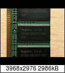
Aeneon 1 GB, CE-5
Aeneon 512 MB, CE-5
Aeneon 512 MB, BE-5
Aeneon 256 MB, CE-6
HYNIX 1 GB, D43
NANYA 512 MB, B-5T
NANYA 256 MB, C-5T
Aeneon CE-5 1024 MB Riegel Nr. 4 auf DFI Lanparty nF4 Ultra-D Sockel 939
Aeneon AED760UD00-500C98X
double sided, 45. KW 2008, Aufdruck AED93T500 C -> Aeneon CE-5
Spezifikation: 200 MHz @ 3-3-3-8 @ 2,50 Volt
Möglich:
-> CL2 / CL2,5 / CL3
Nicht möglich:
-> tRCD <3
SuperPi 1M Testdurchlauf (alle Subtimings auf "Auto")
2,0-3-2-5 @ 235 MHz @ 2,70 v
2,5-3-3-6 @ 265 MHz @ 2,70 v
3,0-3-2-8 @ 250 MHz @ 2,50 v
3,0-3-3-8 @ 295 MHz @ 2,70 v
3,0-4-3-8 @ 295 MHz @ 2,70 v
3,0-4-4-8 @ 295 MHz @ 2,70 v
Dieser Riegel skaliert sehr gut mit dem Takt. Bei CL3 ist es mit langsamen Timings egal, die 295 MHz sind immer drin. Leider knapp an den 300 MHz gescheitert.

Aeneon CE-5 1024 MB Riegel auf ASRock K7NF2-RAID Sockel 462
Aeneon AED760UD00-500 C98X
double sided, 51. KW 2007, Aufdruck AED93T500 C -> Aeneon CE-5
Spezifikation: 200 MHz @ 3-3-3-8 @ 2,50 Volt
Möglich:
-> CL2 / CL2,5 / CL3
Nicht möglich:
-> tRCD <3
SuperPi 1M Testdurchlauf (Subtimings 3-4-4-4-3-4-5)
2,0-3-2-11 @ 220 MHz @ 2,80 v
2,5-3-2-11 @ 250 MHz @ 2,80 v
3,0-3-2-11 @ 264* MHz @ 2,80 v
*= 264MHz ist board limit.
Aeneon 512 MB, CE-5
Aeneon CE-5 512 MB Riegel Nr. 1 auf DFI Lanparty nF4 Ultra-D Sockel 939
AED660UD00-500C88M
double sided, 26. KW 2007, Aufdruck AED83T500 C4 -> Aeneon CE-5
Spezifikation: 200 MHz @ 3-3-3-8 @ 2,50 Volt
Möglich:
-> CL2 / CL2,5 / CL3
Nicht möglich:
-> tRCD <3
SuperPi 1M Testdurchlauf (alle Subtimings auf "Auto")
2,0-3-2-5 @ 210 MHz @ 2,50 v
2,0-3-3-5 @ 210 MHz @ 2,50 v
2,5-3-2-5 @ 210 MHz @ 2,50 v
2,5-3-3-6 @ 210 MHz @ 2,50 v
3,0-3-3-8 @ 210 MHz @ 2,50 v
Dieser Riegel gibt mir Rätsel auf. Macht mit allen Timings bei 2,50 v die 210 MHz, aber keinen MHz mehr.

Aeneon CE-5 512 MB Riegel Nr. 3 auf DFI Lanparty nF4 Ultra-D Sockel 939
OCZ OCZ400512PF
double sided, 26. KW 2005, Aufdruck AED83T500 C -> Aeneon CE-5
Spezifikation: 200 MHz @ 2,5-3-3-6 @ 2,50 Volt
Möglich:
-> CL2 / CL2,5 / CL3
Nicht möglich:
-> tRCD <3
SuperPi 1M Testdurchlauf (alle Subtimings auf "Auto")
2,0-3-2-5 @ 230 MHz @ 2,60 v
2,0-3-3-5 @ 230 MHz @ 2,50 v
3,0-3-2-5 @ 230 MHz @ 2,50 v
3,0-4-4-8 @ 230 MHz @ 2,50 v
Der OCZ-Riegel ist zwar von Haus aus mit schnelleren Timings durch OCZ spezifiziert, allerdings macht der bei 230 MHz zu, egal bei welchen Timings. Mit den schärfsten Latenzen werden 2,60 v benötigt.

Aeneon CE-5 512 MB Riegel Nr. 7 auf DFI Lanparty nF4 Ultra-D Sockel 939
Aeneon AED660UD00-500C98Y
single sided, 38. KW 2008, Aufdruck AED93T500 C -> Aeneon CE-5
Spezifikation: 200 MHz @ 3-3-3-8 @ 2,50 Volt
Möglich:
-> CL2 / CL2,5 / CL3
Nicht möglich:
-> tRCD <3
SuperPi 1M Testdurchlauf (alle Subtimings auf "Auto")
2,0-3-2-5 @ 235 MHz @ 2,80 v
2,0-3-3-5 @ 235 MHz @ 2,70 v
2,5-3-3-6 @ 265 MHz @ 2,80 v
3,0-3-3-8 @ 275 MHz @ 2,60 v
3,0-4-4-8 @ 275 MHz @ 2,50 v
Dieser Riegel skaliert mit der Spannung recht gut, braucht aber mit den schärfsten Timings bereits 2,80 v im Gegensatz zum Riegel Nr. 3. Keine Limitierung beim Takt, kann an der Bauart "single sided" liegen.

Aeneon CE-5 512 MB Riegel Nr. 9 auf DFI Lanparty nF4 Ultra-D Sockel 939
OCZ OCZ4001024PFDC-K
double sided, 28. KW 2005, Aufdruck AED83T500 C -> Aeneon CE-5
Spezifikation: 200 MHz @ 2,5-3-3-6 @ 2,50 Volt
Möglich:
-> CL2 / CL2,5 / CL3
Nicht möglich:
-> tRCD <3
SuperPi 1M Testdurchlauf (alle Subtimings auf "Auto")
2,0-3-2-5 @ 220 MHz @ 2,50 v
2,0-3-3-5 @ 220 MHz @ 2,50 v
2,5-3-3-6 @ 220 MHz @ 2,50 v
3,0-3-3-8 @ 220 MHz @ 2,50 v
3,0-4-4-8 @ 220 MHz @ 2,50 v
Dieser OCZ-Riegel macht bei 220 MHz dicht und reagiert überhaupt nicht auf Spannung. Was es so alles gibt

Aeneon CE-5 512 MB Riegel Nr. 8 auf DFI Lanparty nF4 Ultra-D Sockel 939
PNY 6464WQDXA8G17
double sided, 32. KW 2007, Aufdruck AED83T500 C5 -> Aeneon CE-5
Spezifikation: 200 MHz @ 3-3-3-8 @ 2,50 Volt
Möglich:
-> CL2 / CL2,5 / CL3
Nicht möglich:
-> tRCD <3
SuperPi 1M Testdurchlauf (alle Subtimings auf "Auto")
2,0-3-2-5 @ 220 MHz @ 2,50 v
2,0-3-3-5 @ 220 MHz @ 2,50 v
2,5-3-3-6 @ 220 MHz @ 2,50 v
3,0-3-3-8 @ 220 MHz @ 2,50 v
3,0-4-4-8 @ 220 MHz @ 2,50 v
Gleiches Spiel wie bei den OCZ. Bei 220 MHz ist Schluss

Aeneon CE-5 512 MB Riegel Nr. 6 auf DFI Lanparty nF4 Ultra-D Sockel 939
Aeneon AED660UD00-500C88X
double sided, 44. KW 2005, Aufdruck AED83T500 C -> Aeneon CE-5
Spezifikation: 200 MHz @ 3-3-3-8 @ 2,50 Volt
Möglich:
-> CL2 / CL2,5 / CL3
Nicht möglich:
-> tRCD <3
SuperPi 1M Testdurchlauf (alle Subtimings auf "Auto")
2,0-3-2-5 @ 210 MHz @ 2,50 v
2,0-3-3-5 @ 210 MHz @ 2,50 v
2,5-3-3-6 @ 210 MHz @ 2,50 v
3,0-3-3-8 @ 210 MHz @ 2,50 v
3,0-4-4-8 @ 210 MHz @ 2,50 v
Diese Riegel sind ja wirklich das Letzte. Da geht wirklich nichts...") Diesen Riegel habe ich genau 2x, brauche also seinen Bruder nicht mal Testen.
Diesen Riegel habe ich genau 2x, brauche also seinen Bruder nicht mal Testen.
Aeneon AED660UD00-500C88X
double sided, 44. KW 2005, Aufdruck AED83T500 C -> Aeneon CE-5
Spezifikation: 200 MHz @ 3-3-3-8 @ 2,50 Volt
Möglich:
-> CL2 / CL2,5 / CL3
Nicht möglich:
-> tRCD <3
SuperPi 1M Testdurchlauf (alle Subtimings auf "Auto")
2,0-3-2-5 @ 210 MHz @ 2,50 v
2,0-3-3-5 @ 210 MHz @ 2,50 v
2,5-3-3-6 @ 210 MHz @ 2,50 v
3,0-3-3-8 @ 210 MHz @ 2,50 v
3,0-4-4-8 @ 210 MHz @ 2,50 v
Diese Riegel sind ja wirklich das Letzte. Da geht wirklich nichts...
Diesen Riegel habe ich genau 2x, brauche also seinen Bruder nicht mal Testen.
Aeneon 512 MB, BE-5
Aeneon BE-5 512 MB Riegel Nr. 2 auf DFI Lanparty nF4 Ultra-D Sockel 939
Aeneon AED660UD00-500B98X
single sided, 5. KW 2006, Aufdruck AED93T500 B -> Aeneon BE-5
Spezifikation: 200 MHz @ 3-3-3-8 @ 2,50 Volt
Möglich:
-> CL2 / CL2,5 / CL3
Nicht möglich:
-> tRCD <3
SuperPi 1M Testdurchlauf (alle Subtimings auf "Auto")
2,0-3-2-5 @ 205 MHz @ 2,50 v
2,5-3-3-6 @ 230 MHz @ 2,60 v
3,0-3-3-8 @ 230 MHz @ 2,60 v
Dieser BE-5 Riegel läuft recht schlecht und springt nicht auf Spannungserhöhung an.

Aeneon 256 MB, CE-6
Aeneon CE-6 256 MB Riegel Nr. 10 auf DFI Lanparty nF4 Ultra-D Sockel 939
Aeneon AED560UD00-600C88X
single sided, Datum unbekannt, Aufdruck G32Mx8 DDR umgelabelt -> Aeneon CE-6
Spezifikation: 166 MHz @ 2,5-3-3-7 @ 2,50 Volt
Möglich:
-> CL2 / CL2,5 / CL3
Nicht möglich:
-> tRCD <3
SuperPi 1M Testdurchlauf (alle Subtimings auf "Auto")
2,0-3-2-5 @ 210 MHz @ 2,50 v
2,5-3-3-6 @ 210 MHz @ 2,50 v
3,0-3-3-8 @ 210 MHz @ 2,50 v
3,0-4-4-8 @ 210 MHz @ 2,50 v
Dieser Riegel schafft knapp mehr als 200 MHz, reagiert aber überhaupt nicht auf Spannungserhöhung.

Aeneon CE-6 256 MB Riegel auf ASRock K7NF2-RAID Sockel 462
Aeneon AED560UD00-600C88X
single sided, Datum unbekannt, Aufdruck G32Mx8 DDR umgelabelt -> Aeneon CE-6
Spezifikation: 166 MHz @ 2,5-3-3-7 @ 2,50 Volt
Möglich:
-> CL2 / CL2,5 / CL3
Nicht möglich:
-> tRCD <3
SuperPi 1M Testdurchlauf (Subtimings 3-4-4-4-3-4-5)
2,0-3-2-11 @ 200 MHz @ 2,50 v
2,5-3-2-11 @ 225 MHz @ 2,50 v
3,0-3-2-11 @ 230 MHz @ 2,50 v
HYNIX 1 GB, D43
Hynix D D43 1 GB Riegel auf DFI Lanparty nF4 Ultra-D Sockel 939
double sided, 52. KW 2008
Datenblattspezifikation: HY5DU12822DTP-D43 @ 200 MHz @ 3-3-3-x
Möglich:
-> CL2,5 und CL3
-> tRAS 0
-> DRAM Idle Timer 0
Nicht möglich:
-> CL2 bei 200 MHz (Spannung 2,60 v - 3,20 v; kein Booten)
-> tRCD <3
-> rRP <2
SuperPi 1M Testdurchlauf (alle Subtimings auf "Auto")
Fazit:
CL 2,5 geht bis 225 MHz, egal ob mit 3-3-x / 4-3-x oder 4-4-x
CL 3 geht bis 250 MHz, allerdings nur mit tRCD 4
double sided, 52. KW 2008
Datenblattspezifikation: HY5DU12822DTP-D43 @ 200 MHz @ 3-3-3-x

Möglich:
-> CL2,5 und CL3
-> tRAS 0
-> DRAM Idle Timer 0
Nicht möglich:
-> CL2 bei 200 MHz (Spannung 2,60 v - 3,20 v; kein Booten)
-> tRCD <3
-> rRP <2
SuperPi 1M Testdurchlauf (alle Subtimings auf "Auto")
| Cl 2,5 - 3 - 2 - 0 | CL 2,5 - 3 - 3 - 0 | CL 2,5 - 4 - 3 - 0 | CL 2,5 - 4 - 4 - 0 |
200 MHz | 2,60 v | 2,60 v | 2,60 v | 2,60 v |
205 MHz | 2,70 v | 2,60 v | 2,60 v | 2,60 v |
210 MHz | - | 2,60 v | 2,60 v | 2,60 v |
215 MHz | - | 2,60 v | 2,60 v | 2,60 v |
220 MHz | - | 2,80 v | 2,60 v | 2,60 v |
225 MHz | - | 3,00 v | 2,80 v | 2,90 v |
| CL 3,0 - 3 - 2 - 0 | CL 3,0 - 3 - 3 - 0 | CL 3,0 - 4 - 3 - 0 | CL 3,0 - 4 - 4 - 0 |
200 MHz | 2,60 v | 2,60 v | 2,60 v | 2,60 v |
205 MHz | 2,80 v | 2,60 v | 2,60 v | 2,60 v |
210 MHz | - | 2,60 v | 2,60 v | 2,60 v |
215 MHz | - | 2,60 v | 2,60 v | 2,60 v |
220 MHz | - | 2,60 v | 2,60 v | 2,60 v |
225 MHz | - | 2,60 v | 2,60 v | 2,60 v |
230 MHz | - | 2,60 v | 2,60 v | 2,60 v |
235 MHz | - | 2,60 v | 2,60 v | 2,60 v |
240 MHz | - | 2,60 v | 2,60 v | 2,60 v |
245 MHz | - | - | 2,70 v | 2,70 v |
250 MHz | - | - | 2,80 v | 2,80 v |
Fazit:
CL 2,5 geht bis 225 MHz, egal ob mit 3-3-x / 4-3-x oder 4-4-x
CL 3 geht bis 250 MHz, allerdings nur mit tRCD 4

NANYA 512 MB, B-5T
Nanya B-5T 512 MB Riegel Nr. 1 auf DFI Lanparty nF4 Ultra-D Sockel 939
Nanya NT512D64S8HB1G-5T
double sided, 16./20. KW 2004, Aufdruck NT5DS32M8BT-5T -> Nanya B-5T
Spezifikation: 200 MHz @ 3-3-3-8 @ 2,50 Volt
Möglich:
-> CL2,5 / CL3, rRCD + tRP 2
Nicht möglich:
-> CL2
SuperPi 1M Testdurchlauf (alle Subtimings auf "Auto")
2,5-2-2-5 @ 205 MHz @ 2,60 v
2,5-3-3-6 @ 210 MHz @ 2,60 v
3,0-3-2-8 @ 210 MHz @ 2,60 v
3,0-3-3-8 @ 225 MHz @ 2,50 v
Nanya B-5T macht keine CL2, der Rest ist verfügbar, allerdings reagiert der Riegel so gu wie nicht auf Spannungsänderung. Kurios: sobald ich tRCD und tRP auf 2 stelle, bootet Windows immer mit mindestens 2,60 Volt, auch wenn ich nur 2,50 Volt im BIOS eingestellt habe.

NANYA 256 MB, C-5T
Nanya CS-5 256 MB Riegel auf ASRock K7NF2-RAID Sockel 462
Nanya NT256D64S88C0GY-5T
single sided, 07/2006, NT5DS32M8CS-5T [TW]
Spezifikation: 200 MHz @ 3-3-3-8 @ 2,50 Volt
Möglich:
-> CL2 / CL2,5 / CL3
Nicht möglich:
---
SuperPi 32M (Subtimings 3-4-4-4-3-4-5; 4-5-5-5-3-5-6)
2,0-2-2-11 @ 200 MHz @ 2,70 v (2,50V reichen richt)
2,0-3-2-11 @ 225 MHz @ 2,70 v
2,5-3-2-11 @ 251 MHz @ 2,70 v
3,0-3-3-11 @ 263 MHz @ 2,70 v
----
Stand:
#630 (inkl. umgelabelte Chips)
#1050 (ohne umgelabelte Chips)
Versionshistorie:
2/2025:
* Tabellen komplett überarbeitet
* Chips nach Density getrennt
* Bilder fehlen leider (noch) wegen Abload.de shutdown
Anhänge


Zuletzt bearbeitet:

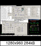
")
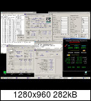
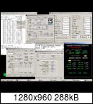
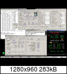
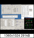
") . Screenshot stable
. Screenshot stable

 Wäre mal eine Projektaufgabe fürs Wochenende, alles mal fein säuberlich dokumentieren.