| Item | Slot #1 | Slot #2 | Slot #3 | Slot #4 |
|---|
| Ram Type | DDR5 | DDR5 | DDR5 | DDR5 |
| Maximum Clock Speed (MHz) | 3100 (XMP) | 3100 (XMP) | 3100 (XMP) | 3100 (XMP) |
| Maximum Transfer Speed (MT/s) | DDR5-6200 | DDR5-6200 | DDR5-6200 | DDR5-6200 |
| Maximum Bandwidth (MB/s) | PC5-24800 | PC5-24800 | PC5-24800 | PC5-24800 |
| Memory Capacity (MB) | 16384 | 16384 | 16384 | 16384 |
| DIMM Temperature | N/A | N/A | N/A | N/A |
| Jedec Manufacture Name | Corsair | Corsair | Corsair | Corsair |
| Search Amazon.com | Search! | Search! | Search! | Search! |
| SPD Revision | 1.0 | 1.0 | 1.0 | 1.0 |
| Registered | No | No | No | No |
| ECC | No | No | No | No |
| On-Die ECC | Yes | Yes | Yes | Yes |
| DIMM Slot # | 1 | 2 | 3 | 4 |
| Manufactured | Week 46 of Year 2024 | Week 11 of Year 2024 | Week 46 of Year 2024 | Week 11 of Year 2024 |
| Module Part # | CMP32GX5M2B6000Z30 | CMP32GX5M2B6000Z30 | CMP32GX5M2B6000Z30 | CMP32GX5M2B6000Z30 |
| Module Revision | 0x0 | 0x0 | 0x0 | 0x0 |
| Module Serial # | 00000000 (029e00244600000000) | 00000000 (029e00241100000000) | 00000000 (029e00244600000000) | 00000000 (029e00241100000000) |
| Module Manufacturing Location | 0 | 0 | 0 | 0 |
| # of Row Addressing Bits | 16 | 16 | 16 | 16 |
| # of Column Addressing Bits | 10 | 10 | 10 | 10 |
| # of Banks | 32 | 32 | 32 | 32 |
| # of Ranks | 1 | 1 | 1 | 1 |
| Device Width in Bits | 8 | 8 | 8 | 8 |
| Bus Width in Bits | 32 | 32 | 32 | 32 |
| Module Voltage | 1.1V | 1.1V | 1.1V | 1.1V |
| CAS Latencies Supported | 22 28 30 32 36 40 42 | 22 28 30 32 36 40 42 | 22 28 30 32 36 40 42 | 22 28 30 32 36 40 42 |
| Timings @ Max Frequency (JEDEC) | 40-40-40-77 | 40-40-40-77 | 40-40-40-77 | 40-40-40-77 |
| Maximum frequency (MHz) | 2400 | 2400 | 2400 | 2400 |
| Maximum Transfer Speed (MT/s) | DDR5-4800 | DDR5-4800 | DDR5-4800 | DDR5-4800 |
| Maximum Bandwidth (MB/s) | PC5-19200 | PC5-19200 | PC5-19200 | PC5-19200 |
| Minimum Clock Cycle Time, tCK (ns) | 0.416 | 0.416 | 0.416 | 0.416 |
| Minimum CAS Latency Time, tAA (ns) | 16.666 | 16.666 | 16.666 | 16.666 |
| Minimum RAS to CAS Delay, tRCD (ns) | 16.666 | 16.666 | 16.666 | 16.666 |
| Minimum Row Precharge Time, tRP (ns) | 16.666 | 16.666 | 16.666 | 16.666 |
| Minimum Active to Precharge Time, tRAS (ns) | 32.000 | 32.000 | 32.000 | 32.000 |
| Minimum Row Active to Row Active Delay, tRRD (ns) | 0.000 | 0.000 | 0.000 | 0.000 |
| Minimum Auto-Refresh to Active/Auto-Refresh Time, tRC (ns) | 48.666 | 48.666 | 48.666 | 48.666 |
| Minimum Auto-Refresh to Active/Auto-Refresh Command Period, tRFC (ns) | 295.000 | 295.000 | 295.000 | 295.000 |
| | | | |
| DDR5 Specific SPD Attributes | | | | |
| Maximum Clock Cycle Time, tCKmax (ns) | 1.010 | 1.010 | 1.010 | 1.010 |
| Write Recovery time (ns) | 30.000 | 30.000 | 30.000 | 30.000 |
| Minimum Auto-Refresh to Active/Auto Refresh Command Period, tRFC2 (ns) | 160.000 | 160.000 | 160.000 | 160.000 |
| Minimum Auto-Refresh to Active/Auto Refresh Command Period, tRFC4 (ns) | 130.000 | 130.000 | 130.000 | 130.000 |
| Minimum Refresh Recovery Delay Time, tRFC1 (ns) | 0.000 | 0.000 | 0.000 | 0.000 |
| Minimum Refresh Recovery Delay Time, tRFC2 (ns) | 0.000 | 0.000 | 0.000 | 0.000 |
| Minimum Refresh Recovery Delay Time, tRFCsb (ns) | 0.000 | 0.000 | 0.000 | 0.000 |
| Module Type | UDIMM | UDIMM | UDIMM | UDIMM |
| Module information SPD revision | 1.0 | 1.0 | 1.0 | 1.0 |
| SPD present | Yes | Yes | Yes | Yes |
| SPD device type | SPD5118 | SPD5118 | SPD5118 | SPD5118 |
| SPD Manufacturer | IDT (Bank: 1, ID: 0xB3) | Montage Technology Group (Bank: 7, ID: 0x32) | IDT (Bank: 1, ID: 0xB3) | Montage Technology Group (Bank: 7, ID: 0x32) |
| PMIC 0 present | Yes | Yes | Yes | Yes |
| PMIC 0 device type | PMIC5100 | PMIC5100 | PMIC5100 | PMIC5100 |
| PMIC 0 Manufacturer | Richtek Power (Bank: 11, ID: 0x8C) | Richtek Power (Bank: 11, ID: 0x8C) | Richtek Power (Bank: 11, ID: 0x8C) | Richtek Power (Bank: 11, ID: 0x8C) |
| PMIC 1 present | No | No | No | No |
| PMIC 1 device type | | | | |
| PMIC 1 Manufacturer | | | | |
| PMIC 2 present | No | No | No | No |
| PMIC 2 device type | | | | |
| PMIC 2 Manufacturer | | | | |
| Thermal Sensor 0 present | No | No | No | No |
| Thermal Sensor 1 present | No | No | No | No |
| Thermal Sensor device type | | | | |
| Thermal Sensor Manufacturer | | | | |
| Module Height (mm) | 46 | 46 | 46 | 46 |
| Module Thickness Front (mm) | 4 | 4 | 4 | 4 |
| Module Thickness Back (mm) | 4 | 4 | 4 | 4 |
| Module Reference Card | Raw Card A Rev. 0 | Raw Card A Rev. 0 | Raw Card A Rev. 0 | Raw Card A Rev. 0 |
| # DRAM Rows | 1 | 1 | 1 | 1 |
| Heat spreader installed | Yes | Yes | Yes | Yes |
| Operating Temperature Range | XT (0 to + 95 �C) | XT (0 to + 95 �C) | XT (0 to + 95 �C) | XT (0 to + 95 �C) |
| Rank Mix | Symmetrical | Symmetrical | Symmetrical | Symmetrical |
| Number of Package Ranks per Channel | 1 | 1 | 1 | 1 |
| Number of Channels per DIMM | 2 | 2 | 2 | 2 |
| Primary bus width per Channel | 32 bits | 32 bits | 32 bits | 32 bits |
| Bus width extension per Channel | 0 bits | 0 bits | 0 bits | 0 bits |
| DRAM Manufacture ID | 173 | 173 | 173 | 173 |
| DRAM Manufacture Bank | 1 | 1 | 1 | 1 |
| DRAM Manufacture Name | SK Hynix | SK Hynix | SK Hynix | SK Hynix |
| DRAM Stepping | 4.1 | 4.1 | 4.1 | 4.1 |
| SDRAM Package Type | Monolithic SDRAM | Monolithic SDRAM | Monolithic SDRAM | Monolithic SDRAM |
| SDRAM Density Per Die | 16Gb | 16Gb | 16Gb | 16Gb |
| SDRAM Bank Groups | 8 | 8 | 8 | 8 |
| SDRAM Banks Per Bank Group | 4 | 4 | 4 | 4 |
| Second SDRAM Package Type | | | | |
| Second SDRAM Density Per Die | | | | |
| Second SDRAM Column Address Bits | | | | |
| Second SDRAM Row Address Bits | | | | |
| Second SDRAM Device Width | | | | |
| Second SDRAM Bank Groups | | | | |
| Second SDRAM Banks Per Bank Group | | | | |
| First SDRAM RFM RAAMMT | 0X (FGR: 0X) | 0X (FGR: 0X) | 0X (FGR: 0X) | 0X (FGR: 0X) |
| First SDRAM RFM RAAIMT | 0 (FGR: 0) | 0 (FGR: 0) | 0 (FGR: 0) | 0 (FGR: 0) |
| First SDRAM RFM Required | no | no | no | no |
| First SDRAM RFM RAA Counter Decrement per REF command | RAAIMT / 2 | RAAIMT / 2 | RAAIMT / 2 | RAAIMT / 2 |
| Second SDRAM RFM RAAMMT | | | | |
| Second SDRAM RFM RAAIMT | | | | |
| Second SDRAM RFM Required | | | | |
| Second SDRAM RFM RAA Counter Decrement per REF command | | | | |
| First SDRAM ARFM Level A RAAMMT | 0X (FGR: 0X) | 0X (FGR: 0X) | 0X (FGR: 0X) | 0X (FGR: 0X) |
| First SDRAM ARFM Level A RAAIMT | 0 (FGR: 0) | 0 (FGR: 0) | 0 (FGR: 0) | 0 (FGR: 0) |
| First SDRAM ARFM Level A supported | no | no | no | no |
| First SDRAM ARFM Level A RAA Counter Decrement per REF command | RAAIMT / 2 | RAAIMT / 2 | RAAIMT / 2 | RAAIMT / 2 |
| Second SDRAM ARFM Level A RAAMMT | | | | |
| Second SDRAM ARFM Level A RAAIMT | | | | |
| Second SDRAM ARFM Level A supported | | | | |
| Second SDRAM ARFM Level A RAA Counter Decrement per REF command | | | | |
| First SDRAM ARFM Level B RAAMMT | 0X (FGR: 0X) | 0X (FGR: 0X) | 0X (FGR: 0X) | 0X (FGR: 0X) |
| First SDRAM ARFM Level B RAAIMT | 0 (FGR: 0) | 0 (FGR: 0) | 0 (FGR: 0) | 0 (FGR: 0) |
| First SDRAM ARFM Level B supported | no | no | no | no |
| First SDRAM ARFM Level B RAA Counter Decrement per REF command | RAAIMT / 2 | RAAIMT / 2 | RAAIMT / 2 | RAAIMT / 2 |
| Second SDRAM ARFM Level B RAAMMT | | | | |
| Second SDRAM ARFM Level B RAAIMT | | | | |
| Second SDRAM ARFM Level B supported | | | | |
| Second SDRAM ARFM Level B RAA Counter Decrement per REF command | | | | |
| First SDRAM ARFM Level C RAAMMT | 0X (FGR: 0X) | 0X (FGR: 0X) | 0X (FGR: 0X) | 0X (FGR: 0X) |
| First SDRAM ARFM Level C RAAIMT | 0 (FGR: 0) | 0 (FGR: 0) | 0 (FGR: 0) | 0 (FGR: 0) |
| First SDRAM ARFM Level C supported | no | no | no | no |
| First SDRAM ARFM Level C RAA Counter Decrement per REF command | RAAIMT / 2 | RAAIMT / 2 | RAAIMT / 2 | RAAIMT / 2 |
| Second SDRAM ARFM Level C RAAMMT | | | | |
| Second SDRAM ARFM Level C RAAIMT | | | | |
| Second SDRAM ARFM Level C supported | | | | |
| Second SDRAM ARFM Level C RAA Counter Decrement per REF command | | | | |
| sPPR Granularity | bank group | bank group | bank group | bank group |
| sPPR Undo/Lock | supported | supported | supported | supported |
| Burst length 32 | not supported | not supported | not supported | not supported |
| MBIST/mPPR | not supported | not supported | not supported | not supported |
| mPPR/hPPR Abort | not supported | not supported | not supported | not supported |
| PASR | not supported | not supported | not supported | not supported |
| DCA Types Supported | Device does not support DCA | Device does not support DCA | Device does not support DCA | Device does not support DCA |
| x4 RMW/ECS Writeback Suppression | not supported | not supported | not supported | not supported |
| x4 RMW/ECS Writeback Suppression MR selector | MR9 | MR9 | MR9 | MR9 |
| Bounded Fault | not supported | not supported | not supported | not supported |
| SDRAM Nominal Voltage, VDDQ | 1.1V | 1.1V | 1.1V | 1.1V |
| SDRAM Nominal Voltage, VPP | 1.8V | 1.8V | 1.8V | 1.8V |
| Cyclical Redundancy Code (CRC) for Base Configuration | 58a2 | c547 | 58a2 | c547 |
| | | | |
| XMP Attributes | | | | |
| XMP version | 3.0 | 3.0 | 3.0 | 3.0 |
| PMIC Vendor ID | 8A8C | 8A8C | 8A8C | 8A8C |
| Number of PMICs on DIMM | 1 | 1 | 1 | 1 |
| PMIC capabilities | | | | |
| PMIC has capabilities for OC functions | No | No | No | No |
| Current PMIC OC is enabled | No | No | No | No |
| PMIC voltage default step size | 5mV | 5mV | 5mV | 5mV |
| OC global reset functions | No | No | No | No |
| Validation and Certification Capabilities | | | | |
| DIMM is self-certified by DIMM vendor | No | No | No | No |
| PMIC Component is validated by Intel AVL level | No | No | No | No |
| XMP revision | 1.2 | 1.2 | 1.2 | 1.2 |
| XMP Profile 1 | | | | |
| Profile name | Profile 1 | Profile 1 | Profile 1 | Profile 1 |
| XMP Certified | No | No | No | No |
| Recommended number of DIMMs per channel | 1 | 1 | 1 | 1 |
| Module VPP voltage | 1.80V | 1.80V | 1.80V | 1.80V |
| Module VDD voltage | 1.40V | 1.40V | 1.40V | 1.40V |
| Module VDDQ voltage | 1.40V | 1.40V | 1.40V | 1.40V |
| Memory Controller voltage | 1.20V | 1.20V | 1.20V | 1.20V |
| Clock speed (MHz) | 3000 | 3000 | 3000 | 3000 |
| Transfer Speed (MT/s) | DDR5-6000 | DDR5-6000 | DDR5-6000 | DDR5-6000 |
| Bandwidth (MB/s) | PC5-24000 | PC5-24000 | PC5-24000 | PC5-24000 |
| Minimum clock cycle time, tCK (ns) | 0.333 | 0.333 | 0.333 | 0.333 |
| Supported CAS latencies | 22 26 28 30 32 36 40 42 46 48 50 54 | 22 26 28 30 32 36 40 42 46 48 50 54 | 22 26 28 30 32 36 40 42 46 48 50 54 | 22 26 28 30 32 36 40 42 46 48 50 54 |
| Minimum CAS latency time, tAA (ns) | 9.990 | 9.990 | 9.990 | 9.990 |
| Minimum RAS to CAS delay time, tRCD (ns) | 11.988 | 11.988 | 11.988 | 11.988 |
| Minimum row precharge time, tRP (ns) | 11.988 | 11.988 | 11.988 | 11.988 |
| Minimum active to precharge time, tRAS (ns) | 25.308 | 25.308 | 25.308 | 25.308 |
| Supported timing at highest clock speed | 30-36-36-76 | 30-36-36-76 | 30-36-36-76 | 30-36-36-76 |
| Minimum Active to Auto-Refresh Delay, tRC (ns) | 37.296 | 37.296 | 37.296 | 37.296 |
| Minimum Write Recovery Time, tWR (ns) | 30.000 | 30.000 | 30.000 | 30.000 |
| Minimum Auto-Refresh to Active/Auto-Refresh Delay, tRFC1 (ns) | 295.000 | 295.000 | 295.000 | 295.000 |
| Minimum Auto-Refresh to Active/Auto-Refresh Delay, tRFC2 (ns) | 160.000 | 160.000 | 160.000 | 160.000 |
| Minimum Auto-Refresh to Active/Auto-Refresh Delay, tRFCsb (ns) | 130.000 | 130.000 | 130.000 | 130.000 |
| Minimum Read to Read Command Delay Time, Same Bank Group, tCCD_L (ns) | 5.000 (8 nCK) | 5.000 (8 nCK) | 5.000 (8 nCK) | 5.000 (8 nCK) |
| Minimum Write to Write Command Delay Time, Same Bank Group, tCCD_L_WR (ns) | 20.000 (32 nCK) | 20.000 (32 nCK) | 20.000 (32 nCK) | 20.000 (32 nCK) |
| Minimum Write to Write Command Delay Time, Second Write not RMW, Same Bank Group, tCCD_L_WR2 (ns) | 10.000 (16 nCK) | 10.000 (16 nCK) | 10.000 (16 nCK) | 10.000 (16 nCK) |
| Minimum Write to Read Command Delay Time, Same Bank Group, tCCD_L_WTR (ns) | 10.000 (16 nCK) | 10.000 (16 nCK) | 10.000 (16 nCK) | 10.000 (16 nCK) |
| Minimum Write to Read Command Delay Time, Different Bank Group, tCCD_S_WTR (ns) | 2.500 (4 nCK) | 2.500 (4 nCK) | 2.500 (4 nCK) | 2.500 (4 nCK) |
| Minimum Active to Active Command Delay Time, Same Bank Group, tRRD_L (ns) | 5.000 (8 nCK) | 5.000 (8 nCK) | 5.000 (8 nCK) | 5.000 (8 nCK) |
| Minimum Read to Precharge Command Delay Time, tRTP (ns) | 7.500 (12 nCK) | 7.500 (12 nCK) | 7.500 (12 nCK) | 7.500 (12 nCK) |
| Minimum Four Activate Window, tFAW (ns) | 10.666 | 10.666 | 10.666 | 10.666 |
| Advanced Memory Overclocking Features | | | | |
| Real-Time Memory Frequency Overclocking | Supported | Supported | Supported | Supported |
| Intel Dynamic Memory Boost | Supported | Supported | Supported | Supported |
| System CMD Rate Mode | 2N | 2N | 2N | 2N |
| Vendor Personality Byte | 0x00 | 0x00 | 0x00 | 0x00 |
| XMP Profile 2 | | | | |
| Profile name | Profile 2 | Profile 2 | Profile 2 | Profile 2 |
| XMP Certified | No | No | No | No |
| Recommended number of DIMMs per channel | 1 | 1 | 1 | 1 |
| Module VPP voltage | 1.80V | 1.80V | 1.80V | 1.80V |
| Module VDD voltage | 1.40V | 1.40V | 1.40V | 1.40V |
| Module VDDQ voltage | 1.40V | 1.40V | 1.40V | 1.40V |
| Memory Controller voltage | 1.20V | 1.20V | 1.20V | 1.20V |
| Clock speed (MHz) | 3100 | 3100 | 3100 | 3100 |
| Transfer Speed (MT/s) | DDR5-6200 | DDR5-6200 | DDR5-6200 | DDR5-6200 |
| Bandwidth (MB/s) | PC5-24800 | PC5-24800 | PC5-24800 | PC5-24800 |
| Minimum clock cycle time, tCK (ns) | 0.322 | 0.322 | 0.322 | 0.322 |
| Supported CAS latencies | 22 26 28 30 32 36 40 42 46 48 50 52 54 56 | 22 26 28 30 32 36 40 42 46 48 50 52 54 56 | 22 26 28 30 32 36 40 42 46 48 50 52 54 56 | 22 26 28 30 32 36 40 42 46 48 50 52 54 56 |
| Minimum CAS latency time, tAA (ns) | 10.304 | 10.304 | 10.304 | 10.304 |
| Minimum RAS to CAS delay time, tRCD (ns) | 12.236 | 12.236 | 12.236 | 12.236 |
| Minimum row precharge time, tRP (ns) | 12.236 | 12.236 | 12.236 | 12.236 |
| Minimum active to precharge time, tRAS (ns) | 25.760 | 25.760 | 25.760 | 25.760 |
| Supported timing at highest clock speed | 32-38-38-80 | 32-38-38-80 | 32-38-38-80 | 32-38-38-80 |
| Minimum Active to Auto-Refresh Delay, tRC (ns) | 37.996 | 37.996 | 37.996 | 37.996 |
| Minimum Write Recovery Time, tWR (ns) | 29.946 | 29.946 | 29.946 | 29.946 |
| Minimum Auto-Refresh to Active/Auto-Refresh Delay, tRFC1 (ns) | 295.000 | 295.000 | 295.000 | 295.000 |
| Minimum Auto-Refresh to Active/Auto-Refresh Delay, tRFC2 (ns) | 160.000 | 160.000 | 160.000 | 160.000 |
| Minimum Auto-Refresh to Active/Auto-Refresh Delay, tRFCsb (ns) | 130.000 | 130.000 | 130.000 | 130.000 |
| Minimum Read to Read Command Delay Time, Same Bank Group, tCCD_L (ns) | 5.000 (8 nCK) | 5.000 (8 nCK) | 5.000 (8 nCK) | 5.000 (8 nCK) |
| Minimum Write to Write Command Delay Time, Same Bank Group, tCCD_L_WR (ns) | 20.000 (32 nCK) | 20.000 (32 nCK) | 20.000 (32 nCK) | 20.000 (32 nCK) |
| Minimum Write to Write Command Delay Time, Second Write not RMW, Same Bank Group, tCCD_L_WR2 (ns) | 10.000 (16 nCK) | 10.000 (16 nCK) | 10.000 (16 nCK) | 10.000 (16 nCK) |
| Minimum Write to Read Command Delay Time, Same Bank Group, tCCD_L_WTR (ns) | 10.000 (16 nCK) | 10.000 (16 nCK) | 10.000 (16 nCK) | 10.000 (16 nCK) |
| Minimum Write to Read Command Delay Time, Different Bank Group, tCCD_S_WTR (ns) | 2.500 (4 nCK) | 2.500 (4 nCK) | 2.500 (4 nCK) | 2.500 (4 nCK) |
| Minimum Active to Active Command Delay Time, Same Bank Group, tRRD_L (ns) | 5.000 (8 nCK) | 5.000 (8 nCK) | 5.000 (8 nCK) | 5.000 (8 nCK) |
| Minimum Read to Precharge Command Delay Time, tRTP (ns) | 7.500 (12 nCK) | 7.500 (12 nCK) | 7.500 (12 nCK) | 7.500 (12 nCK) |
| Minimum Four Activate Window, tFAW (ns) | 10.666 | 10.666 | 10.666 | 10.666 |
| Advanced Memory Overclocking Features | | | | |
| Real-Time Memory Frequency Overclocking | Supported | Supported | Supported | Supported |
| Intel Dynamic Memory Boost | Supported | Supported | Supported | Supported |
| System CMD Rate Mode | 2N | 2N | 2N | 2N |
| Vendor Personality Byte | 0x00 | 0x00 | 0x00 | 0x00 |
| | | | |
| EXPO Attributes | | | | |
| EXPO version | 1.0 | 1.0 | 1.0 | 1.0 |
| PMIC feature support | | | | |
| PMIC 10 mV step size support | No | No | No | No |
| EXPO Profile 1 | | | | |
| DIMMs per channel supported | 1 | 1 | 1 | 1 |
| EXPO Optional Block Support | | | | |
| Block 1 enabled | No | No | No | No |
| SDRAM VDD | 1.40V | 1.40V | 1.40V | 1.40V |
| SDRAM VDDQ | 1.40V | 1.40V | 1.40V | 1.40V |
| SDRAM VPP | 1.80V | 1.80V | 1.80V | 1.80V |
| Clock speed (MHz) | 3000 | 3000 | 3000 | 3000 |
| Transfer Speed (MT/s) | DDR5-6000 | DDR5-6000 | DDR5-6000 | DDR5-6000 |
| Bandwidth (MB/s) | PC5-24000 | PC5-24000 | PC5-24000 | PC5-24000 |
| Minimum clock cycle time, tCK (ns) | 0.333 | 0.333 | 0.333 | 0.333 |
| Minimum CAS latency time, tAA (ns) | 9.990 | 9.990 | 9.990 | 9.990 |
| Minimum RAS to CAS delay time, tRCD (ns) | 11.988 | 11.988 | 11.988 | 11.988 |
| Minimum row precharge time, tRP (ns) | 11.988 | 11.988 | 11.988 | 11.988 |
| Minimum active to precharge time, tRAS (ns) | 25.308 | 25.308 | 25.308 | 25.308 |
| Supported timing at highest clock speed | 30-36-36-76 | 30-36-36-76 | 30-36-36-76 | 30-36-36-76 |
| Minimum Active to Auto-Refresh Delay, tRC (ns) | 37.296 | 37.296 | 37.296 | 37.296 |
| Minimum Write Recovery Time, tWR (ns) | 30.000 | 30.000 | 30.000 | 30.000 |
| Minimum Auto-Refresh to Active/Auto-Refresh Delay, tRFC1 (ns) | 295.000 | 295.000 | 295.000 | 295.000 |
| Minimum Auto-Refresh to Active/Auto-Refresh Delay, tRFC2 (ns) | 160.000 | 160.000 | 160.000 | 160.000 |
| Minimum Auto-Refresh to Active/Auto-Refresh Delay, tRFCsb (ns) | 130.000 | 130.000 | 130.000 | 130.000 |
| Minimum Active to Active Command Delay Time, Same Bank Group, tRRD_L (ns) | 0.000 | 0.000 | 0.000 | 0.000 |
| Minimum Read to Read Command Delay Time, Same Bank Group, tCCD_L (ns) | 0.000 | 0.000 | 0.000 | 0.000 |
| Minimum Write to Write Command Delay Time, Same Bank Group, tCCD_L_WR (ns) | 0.000 | 0.000 | 0.000 | 0.000 |
| Minimum Write to Write Command Delay Time, Second Write not RMW, Same Bank Group, tCCD_L_WR2 (ns) | 0.000 | 0.000 | 0.000 | 0.000 |
| Minimum Four Activate Window, tFAW (ns) | 0.000 | 0.000 | 0.000 | 0.000 |
| Minimum Write to Read Command Delay Time, Same Bank Group, tWTR_L (ns) | 0.000 | 0.000 | 0.000 | 0.000 |
| Minimum Write to Read Command Delay Time, Different Bank Group, tWTR_S (ns) | 0.000 | 0.000 | 0.000 | 0.000 |
| Minimum Read to Precharge Command Delay Time, tRTP (ns) | 0.000 | 0.000 | 0.000 | 0.000 |

")

")


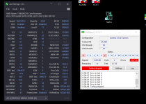
 . procODT jetzt auch wieder AUTO.
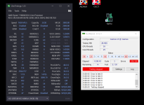