hab ich jetzt auch gefunden, aber danke

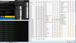
anta777 denke ich mal
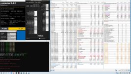
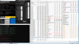
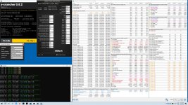
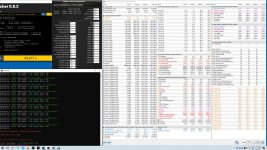
Läuft, bin ich mal gespannt...
Du machst mit dem 1usmus Profil nichts falsch.
Ungenügend wird es, wenn man etwas von einem Programm erwartet, dass überhaupt nicht dafür ausgelegt ist.
TM5 ist da um Powering oder Timing Transition errors zu finden.
Etwas worauf Anta's profil nicht ausgelegt ist und TM5 als solches ebenso nicht.
Wenn man voltage (discharge) stability testen möchte, geht man zu HCI/Karhu ähnlichen Tools.
// GSAT, stressapptest XOR passmark memtest DOS (100% pass)
Solch etwas ist nicht TM5's Aufgabe!
Dein Ergebniss teilt dir nur mit, dass die Spannungen für die RAM Seite aus OK sind.
Ob der Cache und QCLK mithalten kann, bzw Ring & IA supply, ist ein anderes Thema.
I'll do it tomorrow. Count on me.
I was reading your progress with Veii. Very good. Just to know, how do you manage only one value of CTL1? I mean, CMDVrefUp alone? As far as I remember, a value does not modify the other trained ones, so we would have to do tests one by one, is that right? Are these associated with your RTTs? I saw that you used some similar to those from shamino, could it be?
Bit of time off for RL shenanigans, ppls birthdays and socializing

Soo,
CTL1 depends purely on your powering foundation, capacity and board quality
Hence used RTTs + ODTs only work with those slopes
Now each of the 4 values influence it.
If one is bad, all are bad.
But,
There is something you can do like knowledge-guessing and pattern working.
A correct target value for VREF , has to stay within 3 values. Outside of that, it has to align within remain signals.
Its 60 lanes for memory that need to be trained and time align.
DQS & CLK align togher
CMD, CS, CA as DQ (4 links each) then get aligned ontop of each other.
Soo the outcome of this is, that CLK+DQS & DQ's get time aligned and then read or write leveled to be happening at the correct interval.
The biggest challenge is not for those little signals to align, but like BPM sync'ing a song, its for the shifting between and the (how do i say) expanding or thermal skewing/stretching, to not happen.
Hence each and everything has some sort of playroom, but values in between (even between our timings) i mean the micro delays. Those are the biggest challenge to get right.
Back on topic,
Those delays while being completely dependent on your RTT & ODT values, don't have a fixed position.
They mostly scale with the DIMMs density, amount, PCB type (we all are on A0 soo its not too bad) and potentially subzero thermals + Board Layer quality.
They aren't really "trained" values. Else training will take like on AMD a looong time and still doesnt guarantee clean or good training.
There's not really a threshold after when "its a good value". Just success or not, in boot X target.
What we can do, is throwing variables out of the way, and get the lowest functional point done. At whatever
@zebra_hun RTTs are.
Then based on all 4 values we can shift them up and downwards together.
// using bit of logic outside of pure bruteforcing.
Soo focusing on what the Board trains is not important, and will be a bad influence. Placeboo effect.
Of course it would be great to get up with UP + Down, because not only all 4 CTL1's go together, but their distance to the DOWNs will shift.
Tho Down's one can expect that the Board has solid, its rather the starting point that shifts based on strain.
256^4 = 4 294 967 296 combinations :' )
To remove 2/3 of them, as they have 3 step margins.
85^4 = 49 787 136 attempts (better) haha
Out of those, lets say that over half doesnt reach over 15min.
And out of 22mil , maybe 80% don't reach over 2 hours.
Around 4.4mil combinations left . Hahaha
One line out of a million has now been completed.
By the time DDR6 comes out, maybe I'll be done.

Close enough

Once we have all 4 values together, which do not depend too much between Boarddesigns (unless ODM made a design mistake, which's one can expect the apex has an exemplary tracedesign-layout)
We can shift its starting point up and down , to adapt to "whatever RTTs + ODTs are set" at whatever IC Vendor's design.
CTL0 ODT will have the CPU and SA as variables.
But DQ Vref, "the package" delay by clock , has been nailed down. Its floor and ceiling margins too.
It may have a bit of playroom up and down, between 1 DPC and 2 DPC designs, but that part is confidently nailed down.
Gear4 only is not fully checked. Someday (maybe 15th gen?) i'll inspect that part myself too. 10400 Strap is nice and all, but i see only suicide runs, not full stable runs so far.
Shifting clock in runtime (OS) vs actually training at this strap with its delays ~ is a completely different world. Something that we still miss, given (predictive) specification papers only reach 8800MT/s.
Basically long way to go still, soo basically a guaranteed flawed foundation in the current state and room to improve.

I would like to know if there is any information about Data Equialization, and also about DFE Taps and profits. These are in the Gigabyte mobos, but I don't see them in Asus (Taps). Do you know if there is something to read? It's all related and more so at high speeds. I think Asus doesn't want us to go full manual.
Given education belongs free to every individual:
https://oa.mg/ &
https://sci-hub.se/about ~ papers from IEEE Xplore , Harvard, Medical Studies and ongoing
You will find snippets of information between each citations of each researcher groups.
You will not find trade secrets or governmental supported organization papers, but papers by standalone neutral researchers.
But as always, what might be politically fine on one place of the earth, may be restricted on the other
Your milage will vary

The 2ndary part of the message
Data Equialization, and also about DFE Taps and profits. These are in the Gigabyte mobos, but I don't see them in Asus (Taps).
=//=
I think Asus doesn't want us to go full manual.
This is basic power control of whoever silly-head decided that.
There is not much to say, neither a point in it. Its their decision to intentionally remove access to crucial (one of many) parts in DIMM Tuning functionality.
Gladly other Boardpartners haven't taken that silly path yet, but they only provide done presets without much of an explanation.
The current state appears that this is not the Board to do research on. Neither is AMDs locked-up platform. It is what it is.
I can only hope giving it time, this decision will be rethinked by whoever attempts to wall-off research and deny global progression;
DFE is a signal peak filtering algorithm, and reflection filtering algorithm ~ designed specifically for DDR5 high frequency.
It is an interpolated and negative filtering algorithm that tries to flatten down reflections by inserting a negative of a signal with X delay @ Y strength.
Its accurate functionality depends ontop of foundational filtering algorithms, which are CTLE , FFE and couple more


www.overclock.net
Big topic.
RdEqualization i haven't mastered, actually both i haven't
It is a starting and endpoint sync, and like DFE - the values may or may not shift based on Clock and "signal strength"
I'm still a novice

Its just unfortunate the state ASUS (Intel FW-Team) attempts to position themselves.
Give it time and keep on researching neutrally~~
Just uncalculated unfortunate business practices by whoever decided that.
// Some can be intentionally removed to prevent mistakes on "potential snowballing" variables, but i don't know. It's the way of handling it.
// It can be even that not everyone agree's and intentionally forgot to clean it up fully, till the point i shared how to access it. Where now they are gone. Or maybe coincidence as time factor.
Yea there is nothing to say more, it is whatever 🤭


 anta777 denke ich mal


 aber Timings sind doch ok.