Du verwendest einen veralteten Browser. Es ist möglich, dass diese oder andere Websites nicht korrekt angezeigt werden. Du solltest ein Upgrade durchführen oder einen alternativen Browser verwenden.
I couldn't resist, so ordered a 14900 KS. If I am lucky enough it won't have worse IMC. Also hopefully SA bug won't be there.
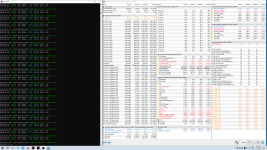
8533 is working fine after a 90 minutes test. I had to push the Vcore for some reason. Maybe my ring or E-cores want more so now my P-core profile is what I shared abvove.
Very strange actually, because I can pass SFT on 57X allcore load, but cannot pass VST and VT3. With the same RAM foundation I can pass VST and VT3 on 58X, which is very strange.
I have no idea what happened tbh. Do you have any idea.
If the KS will be weaker in IMC part I won't keep it.
I think Zeb also bought a new CPU which is much better. He will get my Supercool Gen 12 block too, I will ship it today.
Wenn Du diese Anzeige nicht sehen willst, registriere Dich und/oder logge Dich ein.
I am not up to date what SD tweaked, and how reliable 9903 is to use as "KS MC testing bios"
But as long as everyone uses the same bios, and notes down their V/F curve. I guess~
Not sure, SFT is not Ring heavy. VT3 & VST are.
SFT is very close to an FMA type off P95 small FFT.
I am not up to date what SD tweaked, and how reliable 9903 is to use as "KS MC testing bios"
But as long as everyone uses the same bios, and notes down their V/F curve. I guess~
Not sure, SFT is not Ring heavy. VT3 & VST are.
SFT is very close to an FMA type off P95 small FFT.
After the new block and the chiller. BIOS version doesn't matter, it does the same on every version.
Maybe the curve needs some changes at lower points, tbh I have no idea what happened.
In worst case my ring is degraded a little, but I don't think that could happen with the block change.
Maybe the trained V/F is different with the cold environment.
CMDVREFUP, I'm 99% sure it works fine, but DOWN is 99% sure it doesn't.
I'll check it out, but I'll wait for your advice.
It wasn't a good idea for me to figure out what would be good in an arbitrary style.
This week is now the long week, night shift until Sunday. I finish on Monday morning... 18:00-6:00 am.
In the meantime, here on the Hungarian second-hand market, there were plenty of 14900k high-quality CPUs, everyone wants to buy ks, so I bought a used CPU that was better than mine. I can sell mine later for same money. In some cases, there is a small additional payment to change to the right.
I hope I don't have to start all over again.
Hey! Congrats! I must confess that buying a CPU is like going to the casino. I think many buy it for that adrenaline rush to see if they get a good one. I must confess that the two processors that I bought on Amazon were excellent. I was lucky, but I never buy at launch. Likewise, in my case with an SP105 14900k and a good VF, I think it is more than enough. I should invest in cooling more than in a processor. I wish you luck! You have achieved a lot and have helped many of us.
Hey! Congrats! I must confess that buying a CPU is like going to the casino. I think many buy it for that adrenaline rush to see if they get a good one. I must confess that the two processors that I bought on Amazon were excellent. I was lucky, but I never buy at launch. Likewise, in my case with an SP105 14900k and a good VF, I think it is more than enough. I should invest in cooling more than in a processor. I wish you luck! You have achieved a lot and have helped many of us.
If I would have SP105 like you have, I wouldn't even buy a KS. Your CPU is better than 50% of the KS sold now. My KF is only SP98.
IMC is not bad, that's the only thing I am afraid of.
If I would have SP105 like you have, I wouldn't even buy a KS. Your CPU is better than 50% of the KS sold now. My KF is only SP98.
IMC is not bad, that's the only thing I am afraid of.
Yes, I was lucky really. I could just buy one CPU cause I have lot of custom taxes and shipping cost, so is hit or misss.. But I know I have a good CPU, I just need to work with my VF as you did. Now I{m playing with a 2x24 Xtreem 8200 with deltas. This mem kits are amazing in term of head spreaders, under load, with the same fan on top, I'm below 8~10 degress in comparison with the Gskill. With Karhu or TM5 I'm below 33c with TREFI 131k. In short I will post my first results here Let us know when you receive the new KS!
Hello
I notice them, but i'm not sure i understood.
You found:
70 & things from 110+ seem to work out
It is many combinations, but i think its too early to go with DOWNs
Because you need to isolate it further. Maybe be it with the new CPU @ exactly same voltage targets.
Maybe i don't understand, but i don't see that you are ready to call your minimum values "functional"
But did a nice sweep in shortening the range for you.
The problem that you see with 10 jumps is, while some "holes" values work , some straightout fail to post
It is because you have a range of 3, on hit value which can work and may only fail after long time. That is 4-6 hour mark. 6h is the target.
Its absurdly much work. Even more if this is a personal system. You did quite well actually for the time given
110+ is a good range, compared to old data.
But i'm interested in the ~70 value.
We will need it to fail, this 67-73 range, because it is too far away of 110+
Don't mess with down's till all UPs are ok, i would say
And once all CTL1's are ok, then you first shift them , and only then target RTTs and ODTs.
Needs high thermal testing. (~70°C on Class A, ICs)
If we do start to tune them only on exotic cooling scenarios, our result will not be much different than the APEX are already.
They are configured (mostly) for good scenarios only. I feel it's insufficient, else neither we nor some of the DimmVendors would even bother messing with those options. (far too timeconsuming)
Lets try to not do the same quality work, but better~
No down's for now. Its nowhere near 6h stable.
And if , then there are too many values that work out. Needs maybe higher clock to separate "great" from "optimal".
Once "optimal" is found, its only "optimal" for given RTT+Groups+RONs.
But i'll help here a bit shifting, after we have the data.
Lets see~
I don't think you would. Well you will but i don't think your old data becomes invalid.
Lets say it like that.
If you give the new voltages and remake curve a bit (needs some comment on the low voltage part, but later, post is already huge)
Then RTTs for target DIMMs, and ODT+RON for target Board.
Still should work out.
Are they optimal, absolutely not. Very likely not at all, hence abandoned.
They are not high thermal stable. Just till 48-52° mark.
But if you keep your similar memory cooling, and keep using them while searching for values.
Your old CTL1 data wont become unreproducible, and later you can then shift the targets to new/better RTT & ODTs.
Like i said, i'll help a bit But we need an accurate starting point @ whatever setup.
70-120 range is still too big. Need to invalidate somehow 70 range, to know its 110+ guaranteed.
Else if it stays 67-73 range, then we need more finegranular work and most definitely higher clock.
Because higher range will "just work, till it then doesn't". Lower is better.
Keep same decided SA @ same bios @ same VDDQ-VDDQ delta.
Whatever starting point for VDD2 and VDDQ will be then (will depend on lkg-factor of sample)
The only thing i ask for, to preserve some consistency.
Ein (ROG) Lineup Lesefehler. Angewohnheitsfehler
Den eigentlich gehört STRIX & ROG lineup geteilt.
Ich weiß nicht ob du noch das selbe Board benützt oder ein anderes.
Aber das Strix-E ist 8 Layers.
Das B760i Strix mit 8 layers, failt nach 7200. Und es ist 1DPC.
Wir beide können soweit nicht sagen weswegen, aber ich hatte auf das Hero gehofft, da du mit 7600 kommst.
7600MT/s für 2DPC Boards sind nicht einfach. Ein 7400MT/s cap ist realistisch, und ein 7200MT/s cap ist zu erwarten.
Die Spannungen haben viele namen, jeder nennt sie anders.
VDD(2) & VDDQ auf der CPU Seite. InternalVoltageRegulator (IVR). TX = Transmitter.
und VDD + VDDQ auf der Memory Seite.
SA bleibt SystemAgent.
Sie sollten einfach VDDQ_CPU , VDD2_CPU & VDDQ_MEM, VDD_MEM ~ heißen
Bzw CVDDQ, CVDD2, MVDDQ, MVDD. Viel einfacher und konsistent.
Es ist wie es ist~
You will laugh how amateur I am..
It turns out that the issue was the Vcore on the whole time, not the contact pressure, nor the dimms.
I just set the allcore load to 58x instead of the default 57x and now Y doesn't drop me in a moment...
Maybe the ring or E cores wanted a bit more juice.
So go back and raise AC_LL a little. 58X is okay in VST, but fails in SFT. Doesn't worth the extra juice.
I will write a long post on this topic.
This is long, the tests are also long, sorry, even my post is slow.
One thing is very important.
CMDVrefUP, which we started with, is good.
No one told me, but I started CMDVrefDn, which was a bad idea. Unfortunately, 20-30 minutes of testing is not enough, it is a scam, it deceived me.
You should also know that the auto odt/rtt has never worked for me. I have experienced these values before, without them I could not run the 6-hour race.
Here are my questions:
Is it necessary to do a 6-hour test with VRefUP? I thought I'd find a few more values, then together. This idea is, of course, already a failure at the beginning, because VRefDown does not work unfortunately.
I did a 90-minute test with CMDVRefUP. 90 mins mit 120 VrefUP, aber Down auto
The value was 120 because it made an error below that.
110 still passed the short 20-minute tests, but I wanted to be sure, so I entered 120 and it works.
Got it, I won't change anything else, all voltages will remain as they were.
This is now a quick answer from me, because I wanted you to know, not forgetting, I just need time too.
I like this "work".
In short, the point is, let's check the CMDVref to be 100% sure. 6H long
One thing is very important.
CMDVrefUP, which we started with, is good.
No one told me, but I started CMDVrefDn, which was a bad idea. Unfortunately, 20-30 minutes of testing is not enough, it is a scam, it deceived me.
You should also know that the auto odt/rtt has never worked for me. I have experienced these values before, without them I could not run the 6-hour race.
Here are my questions:
Is it necessary to do a 6-hour test with VRefUP? I thought I'd find a few more values, then together. This idea is, of course, already a failure at the beginning, because VRefDown does not work unfortunately.
I did a 90-minute test with CMDVRefUP. 90 mins mit 120 VrefUP, aber Down auto
The value was 120 because it made an error below that.
You will see the obvious "side-issue" of doing 10 steps only
value -1 to 1 will work, value 3 to 5 will work, value 6-8 will work and 9-11
4 variables which you only test 2 off by going steps of 10. // accepted margins of 3.
// Same as for 8000MT/s CTL0 DQVref can be 170-88 , but also 171-89 or 172-90.
// This took quite some time to figure out, because all of them are correct.
It is good for a short boot test, but it is insufficient for finding the actual minimum value.
Training ontop will already skew the value and then align all of the DQs together. If it doesnt do it, there is no way to run high clock, due to delay between ICs and the amount of traces (60) + dual subchannels.
Shifting only one value, may or may not mess with the others and will have only steps or gears where it can align.
Its not a voltage value to have minimum or ceiling targets. It is an aligned value, but CTl1's are a bit more special. They matter for the strain (on the mem) outside of factoring the trace distance (mainboard) in it.
More delay always will work, till its too much. Ceiling for this one is around the 150 mark.
So we absolutely have to make sure there is nothing interesting in the low 70s range.
Else it starts at 110+. Well all relative really
I think you need to increase strain (higher clock) to start to notice those issues more drastically.
Still at same terts but scaled upwards primaries.
Our 2ndaries and terts are purposely safe.
You need to shift timings @ same voltage because we work with a strain factor.
You should also know that the auto odt/rtt has never worked for me. I have experienced these values before, without them I could not run the 6-hour race.
I know, but i want to figure out whats going on. Its not normal;
Is it mainboard related, is it user related (mounting, tho we improved that part)
Something is off. Is it powersuply and house supply related.
Is it the CPU and potential charred (too much) pads.
Is it a CPU FW bug (can be) when reporting nonsense to training algo.
Is it your Klevvs who maybe run (random) mixed ICs (also seen such practice) ~ soo reporting there nonsense to training algo.
Something is most definitely off.
Just please don't cut IA supply that much.
High or low voltage, whatever.
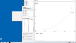
You can shape curve the way it was allowing it to reach high clock, and just "castrate" the boost. Put FMAX lower.
Higher FreqMAX will keep generating further curve points. But lower FMAX will not "mess" with already changed curve.
Your changes on V/F are on SVID level (silly explained). SVID level is ontop of fused curve. Yet FMAX is past all that.
Fused curve is designed based on Intels targets, but the extension and the "lower than usual" ASUS IA_AC programmed, comes afterwards.
The fused curve from Intel-HQ has different characteristics and is tuned based on their Lab PSUs & testing equipment.
It may be rechecked with consumer gear, but it most definitely doesn't align to what Boardpartners design their Boards at.
Soo don't focus on making "new" curves for different clock targets, but make one curve and then improve slowly the freq points.
It will only change "its shape" , aka it will extend upwards, if you allow it to extend (higher FMAX).
it will extend based on the last curve points, aka the shape it follows. Else on lower clock it will not change shape. If it does, its a FW bug.
V/F changes come before FMAX & TVB changes, not after~
// TVB "(asus) voltage optimization" option, comes after SVID preset, not before. Same example.
// V/F point menu is not an ASUS exclusive feature. Its an Intel FW feature. Same for SVID presets, are Intel (alternative) targets ontop of fused curve.
// Why V/F points changes misses on other Boardpartners Bioses is beyond me, but it is what it is;
Capping freq max without doing any V/F changes, will not change the fused curve whatsoever
So also the V/F points have their fixed location, they don't shift just because you messed with FMAX.
I hope that makes sense
Hi! Here they are my results of the new 2x24 Xtreem 8200@1.4v. As I learned from the best, the first thing I did was look for the VDDQ to VDDQ delta. Although the kit comes with 8200 38-49-49-84 @1.4v XMP, I tested the following voltages for 8200:
VDD_mem 1.41 <-> MC 1.42
VDDQ_mem 1.35 <-> VDDQCPU 1.2
SA 1.165
VDDQ Training Disabled - RON Disabled (48-40/40-48). CTL0 DQVrefup/Down
Timings pretty standard. Perhaps I could lower TWR to 24, and increase RDWR to 22
WTRL/S 24-4
I thought that the Mdie were much hotter due to the chip density, in fact the Gskill that I had, whether in 7200 or 8000 Adie 2x16GB, I had a hard time being below 45C while running TM5 or Karhu. Now I'm between 31-33C while running the tests, with the same fan on top. Go down 10C at least. It seems that the heat spreaders are very good. They really surprised me.
My next step is 8400C38. I think all these Mdie 2gen mem kits are the same, the Gskill 8200 1.35/8400 1.4/Viper/Xtreem/Delta. Maybe the SPD writing changed, but from what I saw they are the same chips.
The big question is how to scale. If VDDQ for 8200 is 1.35, which is related to IO or speed, what would be a target for 8400C38? Maintaining the same delta.
Another point is SA. Note that I need a little more at a higher speed. I couldn't go down to 1.14V like I had before, or 1.12 like @tibcsi0407 runs. I wouldn't want to increase too much SA and reduce the deltas.
I think the big step is to undervolt the VFCurve and play with the ACs. It is the step that costs me the most. I'm sure that would give me more headroom for a better mem OC. I don't want to run a lot of CPU OCs. In fact, for now set ICCMAX 400 and PL1/2 300/320W like @zebra_hun
@tibcsi0407 Good luck with your KS order! Excited to see what you end up with. I am VERY much on the fence about getting one. My 14900K is SP100, but still think my IMC is trash. Been messing with VF Curve too much lately, need to get back on the memory OC.
The big question is how to scale. If VDDQ for 8200 is 1.35, which is related to IO or speed, what would be a target for 8400C38? Maintaining the same delta.
I read your post several times.
You consider the frequency reduction to 57 57 56 56 55 55 54 54 instead of the factory default (57 57 60 60 60 57 57 57) to be one of the "main problems".
Yes, in this case I cut the Curve, I don't use the full scale. If I just type it like this, the Curve will be ugly, since its peak starts downward again.
I converted this, it looks good and I think it works well as the 6 H also ran.
Which is why I accept this:
I tried it this way and also with factory settings. If it's wrong, it's wrong either way.
In this case, if I do it wrong, low Vcore for example, I'm doing myself a disservice. I'm actually putting an extra margin of error into the formula.
That's why I don't want to set this up anymore, it's proven, it works.
I call it allcore 54x like 13900k is 55x, KS is 56x and 14900k is 57x.
I think Intel messed this up a lot, they shouldn't have allowed 57. This is problematic for many, many people.
I also think that if I understand correctly, the interval is not as wide at higher frequencies.
So it would be better if I try to make a better ram oc profile, such as 8200C36 or 8400C38. In that case, there might be fewer "good" variations.
I like the allcore 54x, it is also suitable for daily use. Maybe I can do the same as the factory one: 2 cores 60x, 4 cores 58x 6 cores 56x 8 cores 54x. I am concerned about the performance of the Y Cruncher while running, it is ~225 Watts, 1.09V under load. Of course, Amperes also flow less.
PS.:
Heute habe ich um 10 Uhr Termin beim Artz, gerade lauft Test. Hoffentlich wird es nicht froren. Ich habe heute früh länger gelassen.
Neu Info: 110 um 36. min error. Wir sehen, es muss länger testen.
Jetzt lauft 112 über 50 Minute, bis jetzt ohne Problem. Aber ich muss weg, ca. 2 Stunden lasse ich den Rechner aleine.
Hi @Veii, good morning!
After trying several attempts at 8400 I went back to 8200 with the delta I had found and realized that the bitrate was not as consistent. I did a clear CMOS and YC failed in some iterations, from SA 1.165 I tried 1.5, it failed faster, I tried 1.17 and ended up at 1.18. The bitrate still seems a bit inconsistent to me. Since I'm testing 48GB, everything takes longer and I didn't calculate the time correctly. Here I have another run of 8200 with the same delta but SA 1.18. The execution of VST+VT3 should be almost perfect, right? I also tried N63. It didn't fail, but with a bitrate variation (I couldn't get the screenshot).
I'm going to try this one that you just gave me, first 8200 with the parameters you gave me, to see if it works, and then I go to 8400.
This discovery of the deltas is truly incredible. I know it's difficult, but 99.98% use VDDQ Training in Auto, which corrects it. That is, everyone trusts in the BIOS, when we know that retraining errors are huge. I don't know if you remember that you helped me with my Z790 Hero on OCN with 7200 Gskill, I couldn't stabilize it for months. You shared a bios file with VDDQ Training disable and a large delta, and I never had problems again. I really couldn't believe it. Thanks for all the help as always
CMDVRefUP 112 ist die untere Grenze.
110 hat mich am 36. mins Error, 111 geht bestimmt nicht (nie probiert), und 112 ist der Winner. Natuerlich 120 war gut, das ist das 99.99% safety Wert.
[2024/03/22 13:18:15]
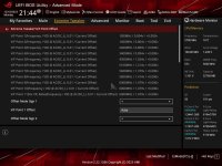
Ai Overclock Tuner [Manual]
BCLK Frequency [100.0000]
PCIE Frequency [100.0000]
Intel(R) Adaptive Boost Technology [Auto]
ASUS MultiCore Enhancement [Enabled – Remove All limits (90°C)]
SVID Behavior [Trained]
BCLK Frequency : DRAM Frequency Ratio [100:100]
Memory Controller : DRAM Frequency Ratio [1:2]
DRAM Frequency [DDR5-8000MHz]
Performance Core Ratio [By Core Usage]
1-Core Ratio Limit [57]
2-Core Ratio Limit [57]
3-Core Ratio Limit [56]
4-Core Ratio Limit [56]
5-Core Ratio Limit [55]
6-Core Ratio Limit [55]
7-Core Ratio Limit [54]
8-Core Ratio Limit [54]
Performance Core0 Specific Ratio Limit [Auto]
Performance Core0 specific Voltage [Auto]
Performance Core1 Specific Ratio Limit [Auto]
Performance Core1 specific Voltage [Auto]
*Performance Core2 Specific Ratio Limit [Auto]
Performance Core2 specific Voltage [Auto]
*Performance Core3 Specific Ratio Limit [Auto]
Performance Core3 specific Voltage [Auto]
Performance Core4 Specific Ratio Limit [Auto]
Performance Core4 specific Voltage [Auto]
Performance Core5 Specific Ratio Limit [Auto]
Performance Core5 specific Voltage [Auto]
Performance Core6 Specific Ratio Limit [Auto]
Performance Core6 specific Voltage [Auto]
Performance Core7 Specific Ratio Limit [Auto]
Performance Core7 specific Voltage [Auto]
Efficient Core Ratio [By Core Usage]
Efficient Turbo Ratio Limit 1 [43]
Efficient Turbo Ratio Cores 1 [Auto]
Efficient Core Group0 Specific Ratio Limit [Auto]
Efficient Core Group0 specific Voltage [Auto]
Efficient Core Group1 Specific Ratio Limit [Auto]
Efficient Core Group1 specific Voltage [Auto]
Efficient Core Group2 Specific Ratio Limit [Auto]
Efficient Core Group2 specific Voltage [Auto]
Efficient Core Group3 Specific Ratio Limit [Auto]
Efficient Core Group3 specific Voltage [Auto]
AVX2 [Auto]
AVX2 Ratio Offset to per-core Ratio Limit [Auto]
AVX2 Voltage Guardband Scale Factor [Auto]
Maximus Tweak [Mode 2]
DRAM CAS# Latency [36]
DRAM RAS# to CAS# Delay Read [46]
DRAM RAS# to CAS# Delay Write [16]
DRAM RAS# PRE Time [46]
DRAM RAS# ACT Time [58]
DRAM Command Rate [2N]
DRAM RAS# to RAS# Delay L [8]
DRAM RAS# to RAS# Delay S [8]
DRAM REF Cycle Time 2 [480]
DRAM REF Cycle Time Same Bank [448]
DRAM Refresh Interval [262143]
DRAM WRITE Recovery Time [24]
DRAM READ to PRE Time [12]
DRAM FOUR ACT WIN Time [32]
DRAM WRITE to READ Delay L [16]
DRAM WRITE to READ Delay S [4]
DRAM CKE Minimum Pulse Width [20]
DRAM Write Latency [34]
Ctl0 dqvrefup [170]
Ctl0 dqvrefdn [88]
Ctl0 dqodtvrefup [Auto]
Ctl0 dqodtvrefdn [Auto]
Ctl1 cmdvrefup [112]
Ctl1 ctlvrefup [Auto]
Ctl1 clkvrefup [Auto]
Ctl1 ckecsvrefup [Auto]
Ctl2 cmdvrefdn [Auto]
Ctl2 ctlvrefdn [Auto]
Ctl2 clkvrefdn [Auto]
Read Equalization RxEq Start Sign [-]
Read Equalization RxEq Start [Auto]
Read Equalization RxEq Stop Sign [-]
Read Equalization RxEq Stop [Auto]
ODT_READ_DURATION [Auto]
ODT_READ_DELAY [Auto]
ODT_WRITE_DURATION [Auto]
ODT_WRITE_DELAY [Auto]
DQ RTT WR [40 DRAM Clock]
DQ RTT NOM RD [40 DRAM Clock]
DQ RTT NOM WR [34 DRAM Clock]
DQ RTT PARK [34 DRAM Clock]
DQ RTT PARK DQS [34 DRAM Clock]
GroupA CA ODT [240 DRAM Clock]
GroupA CS ODT [0 DRAM Clock]
GroupA CK ODT [0 DRAM Clock]
GroupB CA ODT [60 DRAM Clock]
GroupB CS ODT [40 DRAM Clock]
GroupB CK ODT [40 DRAM Clock]
Pull-up Output Driver Impedance [48 DRAM Clock]
Pull-Down Output Driver Impedance [40 DRAM Clock]
DQ RTT WR [40 DRAM Clock]
DQ RTT NOM RD [40 DRAM Clock]
DQ RTT NOM WR [34 DRAM Clock]
DQ RTT PARK [34 DRAM Clock]
DQ RTT PARK DQS [34 DRAM Clock]
GroupA CA ODT [240 DRAM Clock]
GroupA CS ODT [0 DRAM Clock]
GroupA CK ODT [0 DRAM Clock]
GroupB CA ODT [60 DRAM Clock]
GroupB CS ODT [40 DRAM Clock]
GroupB CK ODT [40 DRAM Clock]
Pull-up Output Driver Impedance [40 DRAM Clock]
Pull-Down Output Driver Impedance [48 DRAM Clock]
Round Trip Latency Init Value MC0 CHA [Auto]
Round Trip Latency Max Value MC0 CHA [Auto]
Round Trip Latency Offset Value Mode Sign MC0 CHA [-]
Round Trip Latency Offset Value MC0 CHA [Auto]
Round Trip Latency Init Value MC0 CHB [Auto]
Round Trip Latency Max Value MC0 CHB [Auto]
Round Trip Latency Offset Value Mode Sign MC0 CHB [-]
Round Trip Latency Offset Value MC0 CHB [Auto]
Round Trip Latency Init Value MC1 CHA [Auto]
Round Trip Latency Max Value MC1 CHA [Auto]
Round Trip Latency Offset Value Mode Sign MC1 CHA [-]
Round Trip Latency Offset Value MC1 CHA [Auto]
Round Trip Latency Init Value MC1 CHB [Auto]
Round Trip Latency Max Value MC1 CHB [Auto]
Round Trip Latency Offset Value Mode Sign MC1 CHB [-]
Round Trip Latency Offset Value MC1 CHB [Auto]
Round Trip Latency MC0 CHA R0 [Auto]
Round Trip Latency MC0 CHA R1 [Auto]
Round Trip Latency MC0 CHA R2 [0]
Round Trip Latency MC0 CHA R3 [0]
Round Trip Latency MC0 CHA R4 [0]
Round Trip Latency MC0 CHA R5 [0]
Round Trip Latency MC0 CHA R6 [0]
Round Trip Latency MC0 CHA R7 [0]
Round Trip Latency MC0 CHB R0 [Auto]
Round Trip Latency MC0 CHB R1 [Auto]
Round Trip Latency MC0 CHB R2 [0]
Round Trip Latency MC0 CHB R3 [0]
Round Trip Latency MC0 CHB R4 [0]
Round Trip Latency MC0 CHB R5 [0]
Round Trip Latency MC0 CHB R6 [0]
Round Trip Latency MC0 CHB R7 [0]
Round Trip Latency MC1 CHA R0 [Auto]
Round Trip Latency MC1 CHA R1 [Auto]
Round Trip Latency MC1 CHA R2 [0]
Round Trip Latency MC1 CHA R3 [0]
Round Trip Latency MC1 CHA R4 [0]
Round Trip Latency MC1 CHA R5 [0]
Round Trip Latency MC1 CHA R6 [0]
Round Trip Latency MC1 CHA R7 [0]
Round Trip Latency MC1 CHB R0 [Auto]
Round Trip Latency MC1 CHB R1 [Auto]
Round Trip Latency MC1 CHB R2 [0]
Round Trip Latency MC1 CHB R3 [0]
Round Trip Latency MC1 CHB R4 [0]
Round Trip Latency MC1 CHB R5 [0]
Round Trip Latency MC1 CHB R6 [0]
Round Trip Latency MC1 CHB R7 [0]
Early Command Training [Auto]
SenseAmp Offset Training [Auto]
Early ReadMPR Timing Centering 2D [Auto]
Read MPR Training [Auto]
Receive Enable Training [Auto]
Jedec Write Leveling [Auto]
Early Write Time Centering 2D [Auto]
Early Read Time Centering 2D [Auto]
Write Timing Centering 1D [Auto]
Write Voltage Centering 1D [Auto]
Read Timing Centering 1D [Auto]
Read Timing Centering with JR [Auto]
Dimm ODT Training* [Disabled]
Max RTT_WR [ODT Off]
DIMM RON Training* [Disabled]
Write Drive Strength/Equalization 2D* [Auto]
Write Slew Rate Training* [Auto]
Read ODT Training* [Disabled]
Comp Optimization Training [Auto]
Read Equalization Training* [Auto]
Read Amplifier Training* [Auto]
Write Timing Centering 2D [Auto]
Read Timing Centering 2D [Auto]
Command Voltage Centering [Auto]
Early Command Voltage Centering [Auto]
Write Voltage Centering 2D [Auto]
Read Voltage Centering 2D [Auto]
Late Command Training [Auto]
Round Trip Latency [Auto]
Turn Around Timing Training [Auto]
CMD CTL CLK Slew Rate [Auto]
CMD/CTL DS & E 2D [Auto]
Read Voltage Centering 1D [Auto]
TxDqTCO Comp Training* [Auto]
ClkTCO Comp Training* [Auto]
TxDqsTCO Comp Training* [Auto]
VccDLL Bypass Training [Auto]
CMD/CTL Drive Strength Up/Dn 2D [Auto]
DIMM CA ODT Training [Auto]
PanicVttDnLp Training* [Auto]
Read Vref Decap Training* [Auto]
Vddq Training [Disabled]
Duty Cycle Correction Training [Auto]
Periodic DCC [Auto]
Rank Margin Tool Per Bit [Auto]
DIMM DFE Training [Auto]
EARLY DIMM DFE Training [Auto]
Tx Dqs Dcc Training [Auto]
DRAM DCA Training [Auto]
Write Driver Strength Training [Auto]
Rank Margin Tool [Auto]
Memory Test [Auto]
DIMM SPD Alias Test [Auto]
Receive Enable Centering 1D [Auto]
Retrain Margin Check [Auto]
Write Drive Strength Up/Dn independently [Auto]
LPDDR DqDqs Re-Training [Auto]
Margin Check Limit [Disabled]
tRDRD_sg_Training [Auto]
tRDRD_sg_Runtime [16]
tRDRD_dg_Training [Auto]
tRDRD_dg_Runtime [8]
tRDWR_sg [20]
tRDWR_dg [20]
tWRWR_sg [16]
tWRWR_dg [8]
tWRRD_sg [Auto]
tWRRD_dg [Auto]
tRDRD_dr [0]
tRDRD_dd [0]
tRDWR_dr [0]
tRDWR_dd [0]
tWRWR_dr [0]
tWRWR_dd [0]
tWRRD_dr [0]
tWRRD_dd [0]
tRPRE [Auto]
tWPRE [Auto]
tWPOST [Auto]
tWRPRE [Auto]
tPRPDEN [2]
tRDPDEN [47]
tWRPDEN [Auto]
tCPDED [20]
tREFIX9 [Auto]
Ref Interval [Auto]
tXPDLL [Auto]
tXP [30]
tPPD [2]
tCCD_L_tDLLK [Auto]
tZQCAL [Auto]
tZQCS [Auto]
OREF_RI [Auto]
Refresh Watermarks [High]
Refresh Hp Wm [Auto]
Refresh Panic Wm [Auto]
Refresh Abr Release [Auto]
tXSDLL [2559]
tZQOPER [Auto]
tMOD [Auto]
CounttREFIWhileRefEn [Auto]
HPRefOnMRS [Auto]
SRX Ref Debits [Auto]
RAISE BLK WAIT [Auto]
Ref Stagger En [Auto]
Ref Stagger Mode [Auto]
Disable Stolen Refresh [Auto]
En Ref Type Display [Auto]
Trefipulse Stagger Disable [Auto]
tRPab ext [Auto]
derating ext [Auto]
Allow 2cyc B2B LPDDR [Auto]
tCSH [Auto]
tCSL [Auto]
powerdown Enable [Auto]
idle length [Auto]
raise cke after exit latency [Auto]
powerdown latency [Auto]
powerdown length [Auto]
selfrefresh latency [Auto]
selfrefresh length [Auto]
ckevalid length [Auto]
ckevalid enable [Auto]
idle enable [Auto]
selfrefresh enable [Auto]
Address mirror [Auto]
no gear4 param divide [Auto]
x8 device [Auto]
no gear2 param divide [Auto]
ddr 1dpc split ranks on subch [Auto]
write0 enable [Auto]
MultiCycCmd [Auto]
WCKDiffLowInIdle [Auto]
PBR Disable [Auto]
PBR OOO Dis [Auto]
PBR Disable on hot [Auto]
PBR Exit on Idle Cnt [Auto]
tXSR [519]
Dec tCWL [Auto]
Add tCWL [Auto]
Add 1Qclk delay [Auto]
MRC Fast Boot [Disabled]
MCH Full Check [Auto]
Mem Over Clock Fail Count [3]
Training Profile [Auto]
RxDfe [Auto]
Mrc Training Loop Count [3]
DRAM CLK Period [Auto]
Dll_bwsel [Auto]
Controller 0, Channel 0 Control [Enabled]
Controller 0, Channel 1 Control [Enabled]
Controller 1, Channel 0 Control [Enabled]
Controller 1, Channel 1 Control [Enabled]
MC_Vref0 [Auto]
MC_Vref1 [Auto]
MC_Vref2 [Auto]
Fine Granularity Refresh mode [Auto]
SDRAM Density Per Die [Auto]
SDRAM Banks Per Bank Group [Auto]
SDRAM Bank Groups [Auto]
Dynamic Memory Boost [Disabled]
Realtime Memory Frequency [Disabled]
SA GV [Disabled]
Voltage Monitor [Die Sense]
VRM Initialization Check [Enabled]
CPU Input Voltage Load-line Calibration [Auto]
CPU Load-line Calibration [Level 4:Recommended for OC]
Synch ACDC Loadline with VRM Loadline [Enabled]
CPU Current Capability [Auto]
CPU Current Reporting [Auto]
Core Voltage Suspension [Auto]
CPU VRM Switching Frequency [Auto]
VRM Spread Spectrum [Disabled]
CPU Power Duty Control [Auto]
CPU Power Phase Control [Auto]
CPU Power Thermal Control [125]
CPU Core/Cache Boot Voltage [Auto]
CPU Input Boot Voltage [Auto]
PLL Termination Boot Voltage [Auto]
CPU Standby Boot Voltage [Auto]
Memory Controller Boot Voltage [Auto]
CPU Core Auto Voltage Cap [Auto]
CPU Input Auto Voltage Cap [Auto]
Memory Controller Auto Voltage Cap [Auto]
Fast Throttle Threshold [Auto]
Package Temperature Threshold [Auto]
Regulate Frequency by above Threshold [Auto]
IVR Transmitter VDDQ ICCMAX [Auto]
Unlimited ICCMAX [Auto]
CPU Core/Cache Current Limit Max. [420.00]
Long Duration Package Power Limit [320]
Package Power Time Window [Auto]
Short Duration Package Power Limit [330]
Dual Tau Boost [Disabled]
IA AC Load Line [0.25]
IA DC Load Line [Auto]
IA CEP [Disabled]
SA CEP [Disabled]
IA SoC Iccmax Reactive Protector [Disabled]
Inverse Temperature Dependency Throttle [Auto]
IA VR Voltage Limit [1580]
CPU SVID Support [Auto]
Cache Dynamic OC Switcher [Disabled]
TVB Voltage Optimizations [Disabled]
Enhanced TVB [Disabled]
Overclocking TVB [Disabled]
Overclocking TVB Global Temperature Offset Sign [+]
Overclocking TVB Global Temperature Offset Value [Auto]
Offset Mode Sign 1 [-]
V/F Point 1 Offset [0.01200]
Offset Mode Sign 2 [-]
V/F Point 2 Offset [0.00600]
Offset Mode Sign 3 [+]
V/F Point 3 Offset [0.04500]
Offset Mode Sign 4 [+]
V/F Point 4 Offset [0.04300]
Offset Mode Sign 5 [+]
V/F Point 5 Offset [0.01300]
Offset Mode Sign 6 [-]
V/F Point 6 Offset [0.06200]
Offset Mode Sign 7 [-]
V/F Point 7 Offset [0.15000]
Offset Mode Sign 8 [-]
V/F Point 8 Offset [0.03700]
Offset Mode Sign 9 [-]
V/F Point 9 Offset [0.04500]
Offset Mode Sign 10 [-]
V/F Point 10 Offset [0.04400]
Offset Mode Sign 11 [-]
V/F Point 11 Offset [0.04200]
Initial BCLK Frequency [Auto]
Runtime BCLK OC [Auto]
BCLK Amplitude [Auto]
BCLK Slew Rate [Auto]
BCLK Spread Spectrum [Auto]
Initial PCIE Frequency [Auto]
PCIE/DMI Amplitude [Auto]
PCIE/DMI Slew Rate [Auto]
PCIE/DMI Spread Spectrum [Auto]
Cold Boot PCIE Frequency [Auto]
Realtime Memory Timing [Disabled]
SPD Write Disable [TRUE]
PVD Ratio Threshold [Auto]
SA PLL Frequency Override [Auto]
BCLK TSC HW Fixup [Enabled]
Core Ratio Extension Mode [Disabled]
FLL OC mode [Auto]
UnderVolt Protection [Disabled]
Switch Microcode [Current Microcode]
Xtreme Tweaking [Disabled]
Core PLL Voltage [Auto]
GT PLL Voltage [Auto]
Ring PLL Voltage [Auto]
System Agent PLL Voltage [Auto]
Memory Controller PLL Voltage [Auto]
Efficient-core PLL Voltage [Auto]
CPU 1.8V Small Rail [Auto]
PLL Termination Voltage [Auto]
CPU Standby Voltage [Auto]
PCH 1.05V Voltage [Auto]
PCH 0.82V Voltage [Auto]
CPU Input Voltage Reset Voltage [Auto]
Eventual CPU Input Voltage [Auto]
Eventual Memory Controller Voltage [Auto]
Package Temperature Threshold [Auto]
Regulate Frequency by above Threshold [Auto]
Cooler Efficiency Customize [Keep Training]
Cooler Re-evaluation Algorithm [Normal]
Optimism Scale [100]
Ring Down Bin [Disabled]
Min. CPU Cache Ratio [8]
Max. CPU Cache Ratio [47]
BCLK Aware Adaptive Voltage [Auto]
Actual VRM Core Voltage [Auto]
Global Core SVID Voltage [Auto]
Cache SVID Voltage [Adaptive Mode]
- Offset Mode Sign [-]
- Additional Turbo Mode Cache Voltage [Auto]
- Offset Voltage [0.01000]
CPU L2 Voltage [Adaptive Mode]
- Offset Mode Sign [+]
- Additional Turbo Mode CPU L2 Voltage [Auto]
- Offset Voltage [0.01000]
CPU System Agent Voltage [Manual Mode]
- CPU System Agent Voltage Override [1.12000]
CPU Input Voltage [Auto]
High DRAM Voltage Mode [Enabled]
DRAM VDD Voltage [1.47000]
DRAM VDDQ Voltage [1.41000]
IVR Transmitter VDDQ Voltage [1.21000]
Memory Controller Voltage [1.35000]
MC Voltage Calculation Voltage Base [Auto]
VDD Calculation Voltage Base [Auto]
PMIC Voltages [Sync All PMICs]
SPD HUB VLDO (1.8V) [1.80000]
SPD HUB VDDIO (1.0V) [1.00000]
DRAM VDD Voltage [1.47000]
DRAM VDDQ Voltage [1.41000]
DRAM VPP Voltage [1.81500]
DRAM VDD Switching Frequency [1.50000]
DRAM VDDQ Switching Frequency [1.50000]
DRAM VPP Switching Frequency [1.50000]
DRAM Current Capability [7.87500]
PCI Express Native Power Management [Enabled]
Native ASPM [Disabled]
DMI Link ASPM Control [Disabled]
ASPM [Auto]
L1 Substates [Disabled]
DMI ASPM [Disabled]
DMI Gen3 ASPM [Disabled]
PEG - ASPM [Disabled]
PCI Express Clock Gating [Enabled]
Hardware Prefetcher [Enabled]
Adjacent Cache Line Prefetch [Enabled]
Intel (VMX) Virtualization Technology [Disabled]
Per P-Core Control [Disabled]
Per E-Core Control [Disabled]
Active Performance Cores [All]
Active Efficient Cores [All]
Hyper-Threading [Enabled]
Hyper-Threading of Core 0 [Enabled]
Hyper-Threading of Core 1 [Enabled]
Hyper-Threading of Core 2 [Enabled]
Hyper-Threading of Core 3 [Enabled]
Hyper-Threading of Core 4 [Enabled]
Hyper-Threading of Core 5 [Enabled]
Hyper-Threading of Core 6 [Enabled]
Hyper-Threading of Core 7 [Enabled]
Total Memory Encryption [Disabled]
Legacy Game Compatibility Mode [Disabled]
Boot performance mode [Auto]
Intel(R) SpeedStep(tm) [Enabled]
Intel(R) Speed Shift Technology [Enabled]
Intel(R) Turbo Boost Max Technology 3.0 [Enabled]
Turbo Mode [Enabled]
Acoustic Noise Mitigation [Disabled]
CPU C-states [Auto]
Thermal Monitor [Enabled]
Dual Tau Boost [Disabled]
VT-d [Disabled]
Memory Remap [Enabled]
Enable VMD controller [Enabled]
Map PCIE Storage under VMD [Disabled]
Map SATA Controller under VMD [Disabled]
M.2_1 Link Speed [Auto]
PCIEX16(G5)_1 Link Speed [Auto]
PCIEX16(G5)_2 Link Speed [Auto]
PCIEX1(G4) Link Speed [Auto]
PCIEX4(G4) Link Speed [Auto]
M.2_2 Link Speed [Auto]
DIMM.2_1 Link Speed [Auto]
DIMM.2_2 Link Speed [Auto]
SATA Controller(s) [Enabled]
Aggressive LPM Support [Disabled]
SMART Self Test [Enabled]
M.2_3 [Enabled]
M.2_3 Hot Plug [Disabled]
SATA6G_1 [Enabled]
SATA6G_1 Hot Plug [Disabled]
SATA6G_2 [Enabled]
SATA6G_2 Hot Plug [Disabled]
SATA6G_3 [Enabled]
SATA6G_3 Hot Plug [Disabled]
SATA6G_4 [Enabled]
SATA6G_4 Hot Plug [Disabled]
PTT [Enable]
Intel(R) Dynamic Tuning Technology [Disabled]
PCIE Tunneling over USB4 [Enabled]
Discrete Thunderbolt(TM) Support [Disabled]
Security Device Support [Enable]
SHA256 PCR Bank [Enabled]
Pending operation [None]
Platform Hierarchy [Enabled]
Storage Hierarchy [Enabled]
Endorsement Hierarchy [Enabled]
Physical Presence Spec Version [1.3]
Disable Block Sid [Disabled]
USB Host Controller Support [Disabled]
Password protection of Runtime Variables [Enable]
Above 4G Decoding [Enabled]
Resize BAR Support [Enabled]
SR-IOV Support [Disabled]
Legacy USB Support [Enabled]
XHCI Hand-off [Enabled]
SanDisk [Auto]
LAN_U32G2_1 [Enabled]
U32G1_E5 [Enabled]
U32G1_E6 [Enabled]
U32G1_E7 [Enabled]
U32G1_E8 [Enabled]
U32G2X2_C3 [Enabled]
U32G2_5 [Enabled]
U32G2_6 [Enabled]
U32G2_7 [Enabled]
U32G2_P8 [Enabled]
U32G2X2_C9 [Enabled]
U32G1_E1 [Enabled]
U32G1_E2 [Enabled]
U32G1_E3 [Enabled]
U32G1_E4 [Enabled]
Network Stack [Disabled]
Device [N/A]
Restore AC Power Loss [Power Off]
Max Power Saving [Disabled]
ErP Ready [Disabled]
Power On By PCI-E [Disabled]
Power On By RTC [Disabled]
USB Audio [Enabled]
Intel LAN [Enabled]
USB power delivery in Soft Off state (S5) [Disabled]
Connectivity mode (Wi-Fi & Bluetooth) [Disabled]
When system is in working state [All On]
Q-Code LED Function [Auto]
When system is in sleep, hibernate or soft off states [All On]
M.2_2 Configuration [Auto]
ASMedia USB 3.2 Controller_U32G1_E12 [Enabled]
ASMedia USB 3.2 Controller_U32G1_E34 [Enabled]
GNA Device [Disabled]
ASMedia Storage Controller [Enabled]
Windows Hot-plug Notification [Disabled]
ASPM Support [Disabled]
CPU Temperature [Monitor]
CPU Package Temperature [Monitor]
MotherBoard Temperature [Monitor]
VRM Temperature [Monitor]
Chipset Temperature [Monitor]
T_Sensor Temperature [Monitor]
DIMM.2 Sensor 1 Temperature [Monitor]
DIMM.2 Sensor 2 Temperature [Monitor]
Water In T Sensor Temperature [Monitor]
Water Out T Sensor Temperature [Monitor]
DIMM A1 Temperature [Monitor]
DIMM B1 Temperature [Monitor]
CPU Fan Speed [Monitor]
CPU Optional Fan Speed [Monitor]
Chassis Fan 1 Speed [Monitor]
Chassis Fan 2 Speed [Monitor]
Chassis Fan 3 Speed [Monitor]
Water Pump+ Speed [Monitor]
AIO Pump Speed [Monitor]
Flow Rate [Monitor]
CPU Core Voltage [Monitor]
12V Voltage [Monitor]
5V Voltage [Monitor]
3.3V Voltage [Monitor]
Memory Controller Voltage [Monitor]
CPU Fan Q-Fan Control [DC Mode]
CPU Fan Profile [Standard]
CPU Fan Q-Fan Source [CPU]
CPU Fan Step Up [Level 0]
CPU Fan Step Down [Level 4]
CPU Fan Speed Low Limit [200 RPM]
Chassis Fan 1 Q-Fan Control [Auto Detect]
Chassis Fan 1 Profile [Standard]
Chassis Fan 1 Q-Fan Source [CPU]
Chassis Fan 1 Step Up [Level 0]
Chassis Fan 1 Step Down [Level 0]
Chassis Fan 1 Speed Low Limit [200 RPM]
Chassis Fan 2 Q-Fan Control [PWM Mode]
Chassis Fan 2 Profile [Standard]
Chassis Fan 2 Q-Fan Source [Chipset]
Chassis Fan 2 Step Up [Level 0]
Chassis Fan 2 Step Down [Level 4]
Chassis Fan 2 Speed Low Limit [200 RPM]
Chassis Fan 3 Q-Fan Control [DC Mode]
Chassis Fan 3 Profile [Silent]
Chassis Fan 3 Q-Fan Source [CPU]
Chassis Fan 3 Step Up [Level 0]
Chassis Fan 3 Step Down [Level 0]
Chassis Fan 3 Speed Low Limit [200 RPM]
Water Pump+ Q-Fan Control [PWM Mode]
Water Pump+ Profile [Manual]
Water Pump+ Q-Fan Source [CPU]
Water Pump+ Step Up [Level 0]
Water Pump+ Step Down [Level 4]
Water Pump+ Speed Low Limit [Ignore]
Water Pump+ Point4 Temperature [70]
Water Pump+ Point4 Duty Cycle (%) [100]
Water Pump+ Point3 Temperature [50]
Water Pump+ Point3 Duty Cycle (%) [85]
Water Pump+ Point2 Temperature [40]
Water Pump+ Point2 Duty Cycle (%) [80]
Water Pump+ Point1 Temperature [25]
Water Pump+ Point1 Duty Cycle (%) [60]
AIO Pump Q-Fan Control [Auto Detect]
AIO Pump Profile [Full Speed]
CPU Temperature LED Switch [Enabled]
Launch CSM [Disabled]
OS Type [Other OS]
Secure Boot Mode [Custom]
Fast Boot [Disabled]
Boot Logo Display [Auto]
POST Delay Time [3 sec]
Bootup NumLock State [On]
Wait For 'F1' If Error [Enabled]
Option ROM Messages [Force BIOS]
Interrupt 19 Capture [Disabled]
AMI Native NVMe Driver Support [Enabled]
Setup Mode [Advanced Mode]
Boot Sector (MBR/GPT) Recovery Policy [Local User Control]
Next Boot Recovery Action [Skip]
BIOS Image Rollback Support [Enabled]
Publish HII Resources [Disabled]
Flexkey [Safe Boot]
Setup Animator [Disabled]
Load from Profile [1]
Profile Name [8000P54RTTs]
Save to Profile [1]
DIMM Slot Number [DIMM_A1]
Download & Install ARMOURY CRATE app [Disabled]
Download & Install MyASUS service & app [Disabled]
Mir reicht das 7600er 😉 Hab ja auch noch das von Snakeeyes genommen.
Kämpfe gerade mit dem Gigabyte Pro X, da läuft weder das 7600er, noch das 7800er mit dem Xmp Profil out of the Box, trotz QVL.
Bin ich ehrlich gesagt etwas enttäuscht.
Das Colorful hat das 7800er ohne Murren genommen und lief direkt fehlerfrei.
CMDVRefUP 112 ist die untere Grenze.
110 hat mich am 36. mins Error, 111 geht bestimmt nicht (nie probiert), und 112 ist der Winner. Natuerlich 120 war gut, das ist das 99.99% safety Wert.
[2024/03/22 13:18:15]
Ai Overclock Tuner [Manual]
BCLK Frequency [100.0000]
PCIE Frequency [100.0000]
Intel(R) Adaptive Boost Technology [Auto]
ASUS MultiCore Enhancement [Enabled – Remove All limits (90°C)]
SVID Behavior [Trained]
BCLK Frequency : DRAM Frequency Ratio [100:100]
Memory Controller : DRAM Frequency Ratio [1:2]
DRAM Frequency [DDR5-8000MHz]
Performance Core Ratio [By Core Usage]
1-Core Ratio Limit [57]
2-Core Ratio Limit [57]
3-Core Ratio Limit [56]
4-Core Ratio Limit [56]
5-Core Ratio Limit [55]
6-Core Ratio Limit [55]
7-Core Ratio Limit [54]
8-Core Ratio Limit [54]
Performance Core0 Specific Ratio Limit [Auto]
Performance Core0 specific Voltage [Auto]
Performance Core1 Specific Ratio Limit [Auto]
Performance Core1 specific Voltage [Auto]
*Performance Core2 Specific Ratio Limit [Auto]
Performance Core2 specific Voltage [Auto]
*Performance Core3 Specific Ratio Limit [Auto]
Performance Core3 specific Voltage [Auto]
Performance Core4 Specific Ratio Limit [Auto]
Performance Core4 specific Voltage [Auto]
Performance Core5 Specific Ratio Limit [Auto]
Performance Core5 specific Voltage [Auto]
Performance Core6 Specific Ratio Limit [Auto]
Performance Core6 specific Voltage [Auto]
Performance Core7 Specific Ratio Limit [Auto]
Performance Core7 specific Voltage [Auto]
Efficient Core Ratio [By Core Usage]
Efficient Turbo Ratio Limit 1 [43]
Efficient Turbo Ratio Cores 1 [Auto]
Efficient Core Group0 Specific Ratio Limit [Auto]
Efficient Core Group0 specific Voltage [Auto]
Efficient Core Group1 Specific Ratio Limit [Auto]
Efficient Core Group1 specific Voltage [Auto]
Efficient Core Group2 Specific Ratio Limit [Auto]
Efficient Core Group2 specific Voltage [Auto]
Efficient Core Group3 Specific Ratio Limit [Auto]
Efficient Core Group3 specific Voltage [Auto]
AVX2 [Auto]
AVX2 Ratio Offset to per-core Ratio Limit [Auto]
AVX2 Voltage Guardband Scale Factor [Auto]
Maximus Tweak [Mode 2]
DRAM CAS# Latency [36]
DRAM RAS# to CAS# Delay Read [46]
DRAM RAS# to CAS# Delay Write [16]
DRAM RAS# PRE Time [46]
DRAM RAS# ACT Time [58]
DRAM Command Rate [2N]
DRAM RAS# to RAS# Delay L [8]
DRAM RAS# to RAS# Delay S [8]
DRAM REF Cycle Time 2 [480]
DRAM REF Cycle Time Same Bank [448]
DRAM Refresh Interval [262143]
DRAM WRITE Recovery Time [24]
DRAM READ to PRE Time [12]
DRAM FOUR ACT WIN Time [32]
DRAM WRITE to READ Delay L [16]
DRAM WRITE to READ Delay S [4]
DRAM CKE Minimum Pulse Width [20]
DRAM Write Latency [34]
Ctl0 dqvrefup [170]
Ctl0 dqvrefdn [88]
Ctl0 dqodtvrefup [Auto]
Ctl0 dqodtvrefdn [Auto]
Ctl1 cmdvrefup [112]
Ctl1 ctlvrefup [Auto]
Ctl1 clkvrefup [Auto]
Ctl1 ckecsvrefup [Auto]
Ctl2 cmdvrefdn [Auto]
Ctl2 ctlvrefdn [Auto]
Ctl2 clkvrefdn [Auto]
Read Equalization RxEq Start Sign [-]
Read Equalization RxEq Start [Auto]
Read Equalization RxEq Stop Sign [-]
Read Equalization RxEq Stop [Auto]
ODT_READ_DURATION [Auto]
ODT_READ_DELAY [Auto]
ODT_WRITE_DURATION [Auto]
ODT_WRITE_DELAY [Auto]
DQ RTT WR [40 DRAM Clock]
DQ RTT NOM RD [40 DRAM Clock]
DQ RTT NOM WR [34 DRAM Clock]
DQ RTT PARK [34 DRAM Clock]
DQ RTT PARK DQS [34 DRAM Clock]
GroupA CA ODT [240 DRAM Clock]
GroupA CS ODT [0 DRAM Clock]
GroupA CK ODT [0 DRAM Clock]
GroupB CA ODT [60 DRAM Clock]
GroupB CS ODT [40 DRAM Clock]
GroupB CK ODT [40 DRAM Clock]
Pull-up Output Driver Impedance [48 DRAM Clock]
Pull-Down Output Driver Impedance [40 DRAM Clock]
DQ RTT WR [40 DRAM Clock]
DQ RTT NOM RD [40 DRAM Clock]
DQ RTT NOM WR [34 DRAM Clock]
DQ RTT PARK [34 DRAM Clock]
DQ RTT PARK DQS [34 DRAM Clock]
GroupA CA ODT [240 DRAM Clock]
GroupA CS ODT [0 DRAM Clock]
GroupA CK ODT [0 DRAM Clock]
GroupB CA ODT [60 DRAM Clock]
GroupB CS ODT [40 DRAM Clock]
GroupB CK ODT [40 DRAM Clock]
Pull-up Output Driver Impedance [40 DRAM Clock]
Pull-Down Output Driver Impedance [48 DRAM Clock]
Round Trip Latency Init Value MC0 CHA [Auto]
Round Trip Latency Max Value MC0 CHA [Auto]
Round Trip Latency Offset Value Mode Sign MC0 CHA [-]
Round Trip Latency Offset Value MC0 CHA [Auto]
Round Trip Latency Init Value MC0 CHB [Auto]
Round Trip Latency Max Value MC0 CHB [Auto]
Round Trip Latency Offset Value Mode Sign MC0 CHB [-]
Round Trip Latency Offset Value MC0 CHB [Auto]
Round Trip Latency Init Value MC1 CHA [Auto]
Round Trip Latency Max Value MC1 CHA [Auto]
Round Trip Latency Offset Value Mode Sign MC1 CHA [-]
Round Trip Latency Offset Value MC1 CHA [Auto]
Round Trip Latency Init Value MC1 CHB [Auto]
Round Trip Latency Max Value MC1 CHB [Auto]
Round Trip Latency Offset Value Mode Sign MC1 CHB [-]
Round Trip Latency Offset Value MC1 CHB [Auto]
Round Trip Latency MC0 CHA R0 [Auto]
Round Trip Latency MC0 CHA R1 [Auto]
Round Trip Latency MC0 CHA R2 [0]
Round Trip Latency MC0 CHA R3 [0]
Round Trip Latency MC0 CHA R4 [0]
Round Trip Latency MC0 CHA R5 [0]
Round Trip Latency MC0 CHA R6 [0]
Round Trip Latency MC0 CHA R7 [0]
Round Trip Latency MC0 CHB R0 [Auto]
Round Trip Latency MC0 CHB R1 [Auto]
Round Trip Latency MC0 CHB R2 [0]
Round Trip Latency MC0 CHB R3 [0]
Round Trip Latency MC0 CHB R4 [0]
Round Trip Latency MC0 CHB R5 [0]
Round Trip Latency MC0 CHB R6 [0]
Round Trip Latency MC0 CHB R7 [0]
Round Trip Latency MC1 CHA R0 [Auto]
Round Trip Latency MC1 CHA R1 [Auto]
Round Trip Latency MC1 CHA R2 [0]
Round Trip Latency MC1 CHA R3 [0]
Round Trip Latency MC1 CHA R4 [0]
Round Trip Latency MC1 CHA R5 [0]
Round Trip Latency MC1 CHA R6 [0]
Round Trip Latency MC1 CHA R7 [0]
Round Trip Latency MC1 CHB R0 [Auto]
Round Trip Latency MC1 CHB R1 [Auto]
Round Trip Latency MC1 CHB R2 [0]
Round Trip Latency MC1 CHB R3 [0]
Round Trip Latency MC1 CHB R4 [0]
Round Trip Latency MC1 CHB R5 [0]
Round Trip Latency MC1 CHB R6 [0]
Round Trip Latency MC1 CHB R7 [0]
Early Command Training [Auto]
SenseAmp Offset Training [Auto]
Early ReadMPR Timing Centering 2D [Auto]
Read MPR Training [Auto]
Receive Enable Training [Auto]
Jedec Write Leveling [Auto]
Early Write Time Centering 2D [Auto]
Early Read Time Centering 2D [Auto]
Write Timing Centering 1D [Auto]
Write Voltage Centering 1D [Auto]
Read Timing Centering 1D [Auto]
Read Timing Centering with JR [Auto]
Dimm ODT Training* [Disabled]
Max RTT_WR [ODT Off]
DIMM RON Training* [Disabled]
Write Drive Strength/Equalization 2D* [Auto]
Write Slew Rate Training* [Auto]
Read ODT Training* [Disabled]
Comp Optimization Training [Auto]
Read Equalization Training* [Auto]
Read Amplifier Training* [Auto]
Write Timing Centering 2D [Auto]
Read Timing Centering 2D [Auto]
Command Voltage Centering [Auto]
Early Command Voltage Centering [Auto]
Write Voltage Centering 2D [Auto]
Read Voltage Centering 2D [Auto]
Late Command Training [Auto]
Round Trip Latency [Auto]
Turn Around Timing Training [Auto]
CMD CTL CLK Slew Rate [Auto]
CMD/CTL DS & E 2D [Auto]
Read Voltage Centering 1D [Auto]
TxDqTCO Comp Training* [Auto]
ClkTCO Comp Training* [Auto]
TxDqsTCO Comp Training* [Auto]
VccDLL Bypass Training [Auto]
CMD/CTL Drive Strength Up/Dn 2D [Auto]
DIMM CA ODT Training [Auto]
PanicVttDnLp Training* [Auto]
Read Vref Decap Training* [Auto]
Vddq Training [Disabled]
Duty Cycle Correction Training [Auto]
Periodic DCC [Auto]
Rank Margin Tool Per Bit [Auto]
DIMM DFE Training [Auto]
EARLY DIMM DFE Training [Auto]
Tx Dqs Dcc Training [Auto]
DRAM DCA Training [Auto]
Write Driver Strength Training [Auto]
Rank Margin Tool [Auto]
Memory Test [Auto]
DIMM SPD Alias Test [Auto]
Receive Enable Centering 1D [Auto]
Retrain Margin Check [Auto]
Write Drive Strength Up/Dn independently [Auto]
LPDDR DqDqs Re-Training [Auto]
Margin Check Limit [Disabled]
tRDRD_sg_Training [Auto]
tRDRD_sg_Runtime [16]
tRDRD_dg_Training [Auto]
tRDRD_dg_Runtime [8]
tRDWR_sg [20]
tRDWR_dg [20]
tWRWR_sg [16]
tWRWR_dg [8]
tWRRD_sg [Auto]
tWRRD_dg [Auto]
tRDRD_dr [0]
tRDRD_dd [0]
tRDWR_dr [0]
tRDWR_dd [0]
tWRWR_dr [0]
tWRWR_dd [0]
tWRRD_dr [0]
tWRRD_dd [0]
tRPRE [Auto]
tWPRE [Auto]
tWPOST [Auto]
tWRPRE [Auto]
tPRPDEN [2]
tRDPDEN [47]
tWRPDEN [Auto]
tCPDED [20]
tREFIX9 [Auto]
Ref Interval [Auto]
tXPDLL [Auto]
tXP [30]
tPPD [2]
tCCD_L_tDLLK [Auto]
tZQCAL [Auto]
tZQCS [Auto]
OREF_RI [Auto]
Refresh Watermarks [High]
Refresh Hp Wm [Auto]
Refresh Panic Wm [Auto]
Refresh Abr Release [Auto]
tXSDLL [2559]
tZQOPER [Auto]
tMOD [Auto]
CounttREFIWhileRefEn [Auto]
HPRefOnMRS [Auto]
SRX Ref Debits [Auto]
RAISE BLK WAIT [Auto]
Ref Stagger En [Auto]
Ref Stagger Mode [Auto]
Disable Stolen Refresh [Auto]
En Ref Type Display [Auto]
Trefipulse Stagger Disable [Auto]
tRPab ext [Auto]
derating ext [Auto]
Allow 2cyc B2B LPDDR [Auto]
tCSH [Auto]
tCSL [Auto]
powerdown Enable [Auto]
idle length [Auto]
raise cke after exit latency [Auto]
powerdown latency [Auto]
powerdown length [Auto]
selfrefresh latency [Auto]
selfrefresh length [Auto]
ckevalid length [Auto]
ckevalid enable [Auto]
idle enable [Auto]
selfrefresh enable [Auto]
Address mirror [Auto]
no gear4 param divide [Auto]
x8 device [Auto]
no gear2 param divide [Auto]
ddr 1dpc split ranks on subch [Auto]
write0 enable [Auto]
MultiCycCmd [Auto]
WCKDiffLowInIdle [Auto]
PBR Disable [Auto]
PBR OOO Dis [Auto]
PBR Disable on hot [Auto]
PBR Exit on Idle Cnt [Auto]
tXSR [519]
Dec tCWL [Auto]
Add tCWL [Auto]
Add 1Qclk delay [Auto]
MRC Fast Boot [Disabled]
MCH Full Check [Auto]
Mem Over Clock Fail Count [3]
Training Profile [Auto]
RxDfe [Auto]
Mrc Training Loop Count [3]
DRAM CLK Period [Auto]
Dll_bwsel [Auto]
Controller 0, Channel 0 Control [Enabled]
Controller 0, Channel 1 Control [Enabled]
Controller 1, Channel 0 Control [Enabled]
Controller 1, Channel 1 Control [Enabled]
MC_Vref0 [Auto]
MC_Vref1 [Auto]
MC_Vref2 [Auto]
Fine Granularity Refresh mode [Auto]
SDRAM Density Per Die [Auto]
SDRAM Banks Per Bank Group [Auto]
SDRAM Bank Groups [Auto]
Dynamic Memory Boost [Disabled]
Realtime Memory Frequency [Disabled]
SA GV [Disabled]
Voltage Monitor [Die Sense]
VRM Initialization Check [Enabled]
CPU Input Voltage Load-line Calibration [Auto]
CPU Load-line Calibration [Level 4:Recommended for OC]
Synch ACDC Loadline with VRM Loadline [Enabled]
CPU Current Capability [Auto]
CPU Current Reporting [Auto]
Core Voltage Suspension [Auto]
CPU VRM Switching Frequency [Auto]
VRM Spread Spectrum [Disabled]
CPU Power Duty Control [Auto]
CPU Power Phase Control [Auto]
CPU Power Thermal Control [125]
CPU Core/Cache Boot Voltage [Auto]
CPU Input Boot Voltage [Auto]
PLL Termination Boot Voltage [Auto]
CPU Standby Boot Voltage [Auto]
Memory Controller Boot Voltage [Auto]
CPU Core Auto Voltage Cap [Auto]
CPU Input Auto Voltage Cap [Auto]
Memory Controller Auto Voltage Cap [Auto]
Fast Throttle Threshold [Auto]
Package Temperature Threshold [Auto]
Regulate Frequency by above Threshold [Auto]
IVR Transmitter VDDQ ICCMAX [Auto]
Unlimited ICCMAX [Auto]
CPU Core/Cache Current Limit Max. [420.00]
Long Duration Package Power Limit [320]
Package Power Time Window [Auto]
Short Duration Package Power Limit [330]
Dual Tau Boost [Disabled]
IA AC Load Line [0.25]
IA DC Load Line [Auto]
IA CEP [Disabled]
SA CEP [Disabled]
IA SoC Iccmax Reactive Protector [Disabled]
Inverse Temperature Dependency Throttle [Auto]
IA VR Voltage Limit [1580]
CPU SVID Support [Auto]
Cache Dynamic OC Switcher [Disabled]
TVB Voltage Optimizations [Disabled]
Enhanced TVB [Disabled]
Overclocking TVB [Disabled]
Overclocking TVB Global Temperature Offset Sign [+]
Overclocking TVB Global Temperature Offset Value [Auto]
Offset Mode Sign 1 [-]
V/F Point 1 Offset [0.01200]
Offset Mode Sign 2 [-]
V/F Point 2 Offset [0.00600]
Offset Mode Sign 3 [+]
V/F Point 3 Offset [0.04500]
Offset Mode Sign 4 [+]
V/F Point 4 Offset [0.04300]
Offset Mode Sign 5 [+]
V/F Point 5 Offset [0.01300]
Offset Mode Sign 6 [-]
V/F Point 6 Offset [0.06200]
Offset Mode Sign 7 [-]
V/F Point 7 Offset [0.15000]
Offset Mode Sign 8 [-]
V/F Point 8 Offset [0.03700]
Offset Mode Sign 9 [-]
V/F Point 9 Offset [0.04500]
Offset Mode Sign 10 [-]
V/F Point 10 Offset [0.04400]
Offset Mode Sign 11 [-]
V/F Point 11 Offset [0.04200]
Initial BCLK Frequency [Auto]
Runtime BCLK OC [Auto]
BCLK Amplitude [Auto]
BCLK Slew Rate [Auto]
BCLK Spread Spectrum [Auto]
Initial PCIE Frequency [Auto]
PCIE/DMI Amplitude [Auto]
PCIE/DMI Slew Rate [Auto]
PCIE/DMI Spread Spectrum [Auto]
Cold Boot PCIE Frequency [Auto]
Realtime Memory Timing [Disabled]
SPD Write Disable [TRUE]
PVD Ratio Threshold [Auto]
SA PLL Frequency Override [Auto]
BCLK TSC HW Fixup [Enabled]
Core Ratio Extension Mode [Disabled]
FLL OC mode [Auto]
UnderVolt Protection [Disabled]
Switch Microcode [Current Microcode]
Xtreme Tweaking [Disabled]
Core PLL Voltage [Auto]
GT PLL Voltage [Auto]
Ring PLL Voltage [Auto]
System Agent PLL Voltage [Auto]
Memory Controller PLL Voltage [Auto]
Efficient-core PLL Voltage [Auto]
CPU 1.8V Small Rail [Auto]
PLL Termination Voltage [Auto]
CPU Standby Voltage [Auto]
PCH 1.05V Voltage [Auto]
PCH 0.82V Voltage [Auto]
CPU Input Voltage Reset Voltage [Auto]
Eventual CPU Input Voltage [Auto]
Eventual Memory Controller Voltage [Auto]
Package Temperature Threshold [Auto]
Regulate Frequency by above Threshold [Auto]
Cooler Efficiency Customize [Keep Training]
Cooler Re-evaluation Algorithm [Normal]
Optimism Scale [100]
Ring Down Bin [Disabled]
Min. CPU Cache Ratio [8]
Max. CPU Cache Ratio [47]
BCLK Aware Adaptive Voltage [Auto]
Actual VRM Core Voltage [Auto]
Global Core SVID Voltage [Auto]
Cache SVID Voltage [Adaptive Mode]
- Offset Mode Sign [-]
- Additional Turbo Mode Cache Voltage [Auto]
- Offset Voltage [0.01000]
CPU L2 Voltage [Adaptive Mode]
- Offset Mode Sign [+]
- Additional Turbo Mode CPU L2 Voltage [Auto]
- Offset Voltage [0.01000]
CPU System Agent Voltage [Manual Mode]
- CPU System Agent Voltage Override [1.12000]
CPU Input Voltage [Auto]
High DRAM Voltage Mode [Enabled]
DRAM VDD Voltage [1.47000]
DRAM VDDQ Voltage [1.41000]
IVR Transmitter VDDQ Voltage [1.21000]
Memory Controller Voltage [1.35000]
MC Voltage Calculation Voltage Base [Auto]
VDD Calculation Voltage Base [Auto]
PMIC Voltages [Sync All PMICs]
SPD HUB VLDO (1.8V) [1.80000]
SPD HUB VDDIO (1.0V) [1.00000]
DRAM VDD Voltage [1.47000]
DRAM VDDQ Voltage [1.41000]
DRAM VPP Voltage [1.81500]
DRAM VDD Switching Frequency [1.50000]
DRAM VDDQ Switching Frequency [1.50000]
DRAM VPP Switching Frequency [1.50000]
DRAM Current Capability [7.87500]
PCI Express Native Power Management [Enabled]
Native ASPM [Disabled]
DMI Link ASPM Control [Disabled]
ASPM [Auto]
L1 Substates [Disabled]
DMI ASPM [Disabled]
DMI Gen3 ASPM [Disabled]
PEG - ASPM [Disabled]
PCI Express Clock Gating [Enabled]
Hardware Prefetcher [Enabled]
Adjacent Cache Line Prefetch [Enabled]
Intel (VMX) Virtualization Technology [Disabled]
Per P-Core Control [Disabled]
Per E-Core Control [Disabled]
Active Performance Cores [All]
Active Efficient Cores [All]
Hyper-Threading [Enabled]
Hyper-Threading of Core 0 [Enabled]
Hyper-Threading of Core 1 [Enabled]
Hyper-Threading of Core 2 [Enabled]
Hyper-Threading of Core 3 [Enabled]
Hyper-Threading of Core 4 [Enabled]
Hyper-Threading of Core 5 [Enabled]
Hyper-Threading of Core 6 [Enabled]
Hyper-Threading of Core 7 [Enabled]
Total Memory Encryption [Disabled]
Legacy Game Compatibility Mode [Disabled]
Boot performance mode [Auto]
Intel(R) SpeedStep(tm) [Enabled]
Intel(R) Speed Shift Technology [Enabled]
Intel(R) Turbo Boost Max Technology 3.0 [Enabled]
Turbo Mode [Enabled]
Acoustic Noise Mitigation [Disabled]
CPU C-states [Auto]
Thermal Monitor [Enabled]
Dual Tau Boost [Disabled]
VT-d [Disabled]
Memory Remap [Enabled]
Enable VMD controller [Enabled]
Map PCIE Storage under VMD [Disabled]
Map SATA Controller under VMD [Disabled]
M.2_1 Link Speed [Auto]
PCIEX16(G5)_1 Link Speed [Auto]
PCIEX16(G5)_2 Link Speed [Auto]
PCIEX1(G4) Link Speed [Auto]
PCIEX4(G4) Link Speed [Auto]
M.2_2 Link Speed [Auto]
DIMM.2_1 Link Speed [Auto]
DIMM.2_2 Link Speed [Auto]
SATA Controller(s) [Enabled]
Aggressive LPM Support [Disabled]
SMART Self Test [Enabled]
M.2_3 [Enabled]
M.2_3 Hot Plug [Disabled]
SATA6G_1 [Enabled]
SATA6G_1 Hot Plug [Disabled]
SATA6G_2 [Enabled]
SATA6G_2 Hot Plug [Disabled]
SATA6G_3 [Enabled]
SATA6G_3 Hot Plug [Disabled]
SATA6G_4 [Enabled]
SATA6G_4 Hot Plug [Disabled]
PTT [Enable]
Intel(R) Dynamic Tuning Technology [Disabled]
PCIE Tunneling over USB4 [Enabled]
Discrete Thunderbolt(TM) Support [Disabled]
Security Device Support [Enable]
SHA256 PCR Bank [Enabled]
Pending operation [None]
Platform Hierarchy [Enabled]
Storage Hierarchy [Enabled]
Endorsement Hierarchy [Enabled]
Physical Presence Spec Version [1.3]
Disable Block Sid [Disabled]
USB Host Controller Support [Disabled]
Password protection of Runtime Variables [Enable]
Above 4G Decoding [Enabled]
Resize BAR Support [Enabled]
SR-IOV Support [Disabled]
Legacy USB Support [Enabled]
XHCI Hand-off [Enabled]
SanDisk [Auto]
LAN_U32G2_1 [Enabled]
U32G1_E5 [Enabled]
U32G1_E6 [Enabled]
U32G1_E7 [Enabled]
U32G1_E8 [Enabled]
U32G2X2_C3 [Enabled]
U32G2_5 [Enabled]
U32G2_6 [Enabled]
U32G2_7 [Enabled]
U32G2_P8 [Enabled]
U32G2X2_C9 [Enabled]
U32G1_E1 [Enabled]
U32G1_E2 [Enabled]
U32G1_E3 [Enabled]
U32G1_E4 [Enabled]
Network Stack [Disabled]
Device [N/A]
Restore AC Power Loss [Power Off]
Max Power Saving [Disabled]
ErP Ready [Disabled]
Power On By PCI-E [Disabled]
Power On By RTC [Disabled]
USB Audio [Enabled]
Intel LAN [Enabled]
USB power delivery in Soft Off state (S5) [Disabled]
Connectivity mode (Wi-Fi & Bluetooth) [Disabled]
When system is in working state [All On]
Q-Code LED Function [Auto]
When system is in sleep, hibernate or soft off states [All On]
M.2_2 Configuration [Auto]
ASMedia USB 3.2 Controller_U32G1_E12 [Enabled]
ASMedia USB 3.2 Controller_U32G1_E34 [Enabled]
GNA Device [Disabled]
ASMedia Storage Controller [Enabled]
Windows Hot-plug Notification [Disabled]
ASPM Support [Disabled]
CPU Temperature [Monitor]
CPU Package Temperature [Monitor]
MotherBoard Temperature [Monitor]
VRM Temperature [Monitor]
Chipset Temperature [Monitor]
T_Sensor Temperature [Monitor]
DIMM.2 Sensor 1 Temperature [Monitor]
DIMM.2 Sensor 2 Temperature [Monitor]
Water In T Sensor Temperature [Monitor]
Water Out T Sensor Temperature [Monitor]
DIMM A1 Temperature [Monitor]
DIMM B1 Temperature [Monitor]
CPU Fan Speed [Monitor]
CPU Optional Fan Speed [Monitor]
Chassis Fan 1 Speed [Monitor]
Chassis Fan 2 Speed [Monitor]
Chassis Fan 3 Speed [Monitor]
Water Pump+ Speed [Monitor]
AIO Pump Speed [Monitor]
Flow Rate [Monitor]
CPU Core Voltage [Monitor]
12V Voltage [Monitor]
5V Voltage [Monitor]
3.3V Voltage [Monitor]
Memory Controller Voltage [Monitor]
CPU Fan Q-Fan Control [DC Mode]
CPU Fan Profile [Standard]
CPU Fan Q-Fan Source [CPU]
CPU Fan Step Up [Level 0]
CPU Fan Step Down [Level 4]
CPU Fan Speed Low Limit [200 RPM]
Chassis Fan 1 Q-Fan Control [Auto Detect]
Chassis Fan 1 Profile [Standard]
Chassis Fan 1 Q-Fan Source [CPU]
Chassis Fan 1 Step Up [Level 0]
Chassis Fan 1 Step Down [Level 0]
Chassis Fan 1 Speed Low Limit [200 RPM]
Chassis Fan 2 Q-Fan Control [PWM Mode]
Chassis Fan 2 Profile [Standard]
Chassis Fan 2 Q-Fan Source [Chipset]
Chassis Fan 2 Step Up [Level 0]
Chassis Fan 2 Step Down [Level 4]
Chassis Fan 2 Speed Low Limit [200 RPM]
Chassis Fan 3 Q-Fan Control [DC Mode]
Chassis Fan 3 Profile [Silent]
Chassis Fan 3 Q-Fan Source [CPU]
Chassis Fan 3 Step Up [Level 0]
Chassis Fan 3 Step Down [Level 0]
Chassis Fan 3 Speed Low Limit [200 RPM]
Water Pump+ Q-Fan Control [PWM Mode]
Water Pump+ Profile [Manual]
Water Pump+ Q-Fan Source [CPU]
Water Pump+ Step Up [Level 0]
Water Pump+ Step Down [Level 4]
Water Pump+ Speed Low Limit [Ignore]
Water Pump+ Point4 Temperature [70]
Water Pump+ Point4 Duty Cycle (%) [100]
Water Pump+ Point3 Temperature [50]
Water Pump+ Point3 Duty Cycle (%) [85]
Water Pump+ Point2 Temperature [40]
Water Pump+ Point2 Duty Cycle (%) [80]
Water Pump+ Point1 Temperature [25]
Water Pump+ Point1 Duty Cycle (%) [60]
AIO Pump Q-Fan Control [Auto Detect]
AIO Pump Profile [Full Speed]
CPU Temperature LED Switch [Enabled]
Launch CSM [Disabled]
OS Type [Other OS]
Secure Boot Mode [Custom]
Fast Boot [Disabled]
Boot Logo Display [Auto]
POST Delay Time [3 sec]
Bootup NumLock State [On]
Wait For 'F1' If Error [Enabled]
Option ROM Messages [Force BIOS]
Interrupt 19 Capture [Disabled]
AMI Native NVMe Driver Support [Enabled]
Setup Mode [Advanced Mode]
Boot Sector (MBR/GPT) Recovery Policy [Local User Control]
Next Boot Recovery Action [Skip]
BIOS Image Rollback Support [Enabled]
Publish HII Resources [Disabled]
Flexkey [Safe Boot]
Setup Animator [Disabled]
Load from Profile [1]
Profile Name [8000P54RTTs]
Save to Profile [1]
DIMM Slot Number [DIMM_A1]
Download & Install ARMOURY CRATE app [Disabled]
Download & Install MyASUS service & app [Disabled]
Hi @zebra_hun, how are you?
You are doing an incredible job. I would love to know the methodology so I can help. I know that before CMDVRefUp was always used as an entry point, until Veii shared the CTL0 with us. How does the value you discovered help in practice? I don't remember now the influence of CTL1 on the slopes of the curve. Does this value of 112 give you more stability in YC? more consistency?
Thanks for sharing your BIOS file, not only do you have the Cores limited to 54x but you also have PL1/2 with protection, and 420 ICCMAX. You know that I tried with 346W of ICCMAX and that gives me a frequency of 54x or just below, but even with PL1/2 set the thermal throtling triggers me in some core.
Could you share your factory VF Curve with me? Because I want to start working on that, and I would like to have some point of reference. In my case I just have to correct P3, and it undervaults the entire curve. It would help me a lot! (I read the posts from a few months ago with Veii on how to apply VF10, 11, 9 and so on).
On the other hand, I have other questions about your BIOS file, if you have made a small undervolt of your curve, why do you use AC_LL at 0.25? Shouldn't you go up to compensate for the UV? In fact, with everything set to auto (Load Optimized) I have a reading of 0.268 in LLC4 in ACLL with LLC4.
Thank you! And congrats for your great job!
Finally, why do you have a negative svid offset with the VF adjusted?
Mir reicht das 7600er 😉 Hab ja auch noch das von Snakeeyes genommen.
Kämpfe gerade mit dem Gigabyte Pro X, da läuft weder das 7600er, noch das 7800er mit dem Xmp Profil out of the Box, trotz QVL.
Hi @Veii, how are you? I took your recommendations but none of them worked. In fact, what surprised me is that in all cases I had BSOD, perhaps due to such a low SA both in 8000 at 1.12, and in 8400 while maintaining 8400.
For 8000 lowering SA I set the parameters you indicated, it failed with BSOD immediately, then I removed Vref Down, and set CMD
And then 8400, with SA 1.18, changing the primaries to 38-50-50-50-66 and adjusting the powerdowns, I had an immediate BSOD. Then I tried raising SA and lowering the delta, ie SA 1.21 TX 1.3 and so on, up to TX 1.35 and SA 1.25, and you can see that YC starts working, but VST fails. VST indicates SA errors, right? If you update the CTL0 and nothing else.
I'm a bit lost. I have a perception that my SA problem could be fixed with tuning the VF. When you helped me with my Hero, 7200, Deltas, you also shared a VF with me, which worked perfectly on my 13700kf. Then when switching to the Encore, I kept that VF, and achieved 8266 much more stable than my 14900k, which from what I see, is a pretty good sample with SP105 and VF#10 at 1.428V. It can be that? In fact, something that happens to me is that if I put MCE "Enabled Remove all limits" and SVID in Trained (as always) CB15 Extreme or CB24 fails, that is, I lack voltage at some point. I was able to solve it with SVID in Typical Scenario, or else with an SVID offset of 0.02. But I left it back to Trained because I usually don't run those loads.
Finally, I retested my setup on 8200 for 48 2x24Mdie with MVDD 1.44, MVDDQ CVDD2 1.42 CVDDQ 1.2 SA 1.18 with YC for 90 min. I limited PL1/2 to 280/300, ICCMAX 346. With all that, I don't know why, running an average of 75C in the middle of the execution, a core triggers at very high values, maybe I should limit PL1/2 more. But at least it looks like a good fondation.
Mir reicht das 7600er 😉 Hab ja auch noch das von Snakeeyes genommen.
Kämpfe gerade mit dem Gigabyte Pro X, da läuft weder das 7600er, noch das 7800er mit dem Xmp Profil out of the Box, trotz QVL.
Bin ich ehrlich gesagt etwas enttäuscht.
Das Colorful hat das 7800er ohne Murren genommen und lief direkt fehlerfrei.
Hello,
Busy on my way home
Let me respond to everything more difficult when i'm back home and free. I do read it~
Yea i see, but i need to take a closer look.
I would like to understand why you fail at low SA before anything else
If it is due to too high CVDD2 or something else
Your same is not leaky at all, hence lower voltages are required.
And figuring out max runnable delta too, before proceeding further
Before doing the scaling on "sa up delta smaller"
Thanks. These are all attempts to replace "auto". Not so long ago, I also did a 6-hour long test, then it was auto. I would like to know what is the correct value and what is the minimum stable value.
For the CPU topic:
Yes, I have set safety limits for emergencies. I can't reach them, they're kind of guarantees.
320-330W, 420A, 90°C.
I found allcore 54x to be the lowest Vcore where Y Cruncher still works. This is very borderline for me, because sometimes there is a drop to 1.08V, but it is permanently WHEA. 1.09V is the lower limit.
55x requires 1.14-1.15V, the power on that V/F is ~255-260W.
I use Y Cruncher for debugging, and it can find errors even on 54x, the CPU doesn't have to burn.
I monitor the speeds on this frequency, I can compare if by chance what I was doing became worse or slower.
For the topic of voltage regulation:
I keep the dynamic frequency and voltage. I like this.
I don't want to enter or cut fixed values, so I manipulate the V/F Curve.
The upper part is dead, I don't use it. It is essentially the same as the original settings, only lower frequency at lower voltage. I keep this during all the tests, I don't set it to any other value.
Of course, I can restore it at any time if I need it.
I think that many hundreds of hours of Y Cruncher at 57x, over 1.20V, over 320W is not healthy.
I created this temporarily, but I liked it over time. I don't even want 57-58..x for daily use anymore.
AC LL 0.25, yes. I wanted it higher, but i want UV.
Together with curve.
Minus offset by Cache. It was a test, forgot, but now, i don't wanna remove. It is only -0.010V.
I don't wanna touch, because it works fine.
Returning to the test, whether it makes sense, yes, it is useful.
We'll see
Ps:
You can try my V/F offset, it works for u2, but use AC LL 0.20 or less. Your CPU is great.
But better maybe AC LL 0.28 or 0.30, and ac 55x.
AC LL is higher=better.
I will search my V/F curve. Here is in forum.
Here is the VID board, I found it. It's pretty bad. I will replace it with a sp102 next week.
You do it better, since you are at 8200-8400MHz.
It's true, I told the 7200, 7600, and 8000 when I came here that it was impossible with this cpu.
Veii gave me motivation and spirit
PS2:
I'm no expert, but I want something from you.
Sort HWINFO like I did. Unfortunately, it fits in 3 fields, but make the limits visible.
It is also good if the core clock and the effective clock are visible.
It is also useful if you take the screen while running.
I have a kernel power error when I make the wrong curve, the Vcore is low.
By default, you have thermal throttling at 57x, and I can imagine that it throws, the clock jumps, and the Vcore also jumps. Of course, this is an assumption. It is certain that the CPU power supply can be funny if it is bad. He deceives me.
Y2.5b is a quick SA test for me. Very sensitive for Sytem Agent Voltage.
Hello,
Busy on my way home
Let me respond to everything more difficult when i'm back home and free. I do read it~
Yea i see, but i need to take a closer look.
I would like to understand why you fail at low SA before anything else
If it is due to too high CVDD2 or something else
Your same is not leaky at all, hence lower voltages are required.
And figuring out max runnable delta too, before proceeding further
Before doing the scaling on "sa up delta smaller"
Hi @Veii! Thank you! no worries, I imagine you are busy, when you can. In the meantime I keep testing and learning.
Meanwhile, I'm still running test. I guess the delta that I found VDDQ to VDDQ (150mV) it's good, but I need more tunning. Indeed, I just left again TM5 running (I passed 50 cycles, Karhu, you know, I always focus on YC VST+VT3), and just found two errors.
If tWR is to low, could it be that I set 30 instead of 24? Or perhaps I'd need more MVDD..that's regarding eror #9
Regarding error #15, I guess could be vdimm.
I guess what I could fix in timings could be
tRCDWR to 24 to 49.
RRDs/l are right at 12 8
WTRs could be 7, not 4, perhaps is too tight,
RDWR to 22 as spec, instead of 20 for 8200..
Other thing, guessing, is tREFI set to 131071 could be expose more errors.. I always used 65k, but since this mem kit has an incredible headspreader, I could run high refresh interval..
This set has an XMP of 38-48-48-84 at 1.4v.
So, I noted that MVDDQ at 1.35 is enought, perhaps, the CVDDQ could be a littile bit higher, but 150mV is a good target. I had tried with 1.22 TX, but 1.2 seems to be better. Perhaps I should decrease a little that delta.
MVDD to 1.44 for 8200, perhaps is to low, I set it to have 60mV of inmem delta.
CVDD2 to 1.42 perhaps is to much for 8200 or my VF.
I know I'm not far from a good base of 8200. My goal is 8400 efficient, not tight, I mean, with delta, with good SI. You know I don't like records without good foundations.
For example, I tried 8400 with VDDQ Training in Auto, as Asus wants, and with VDD/VDDQ 1.43 I passed TM5, Karhu, but VST failed in the 4th iteration... I think there are many running this "false stability".
I read your post several times.
You consider the frequency reduction to 57 57 56 56 55 55 54 54 instead of the factory default (57 57 60 60 60 57 57 57) to be one of the "main problems".
Yes, in this case I cut the Curve, I don't use the full scale. If I just type it like this, the Curve will be ugly, since its peak starts downward again.
I converted this, it looks good and I think it works well as the 6 H also ran.
Which is why I accept this:
I tried it this way and also with factory settings. If it's wrong, it's wrong either way.
In this case, if I do it wrong, low Vcore for example, I'm doing myself a disservice. I'm actually putting an extra margin of error into the formula.
That's why I don't want to set this up anymore, it's proven, it works.
I call it allcore 54x like 13900k is 55x, KS is 56x and 14900k is 57x.
I think Intel messed this up a lot, they shouldn't have allowed 57. This is problematic for many, many people.
I also think that if I understand correctly, the interval is not as wide at higher frequencies.
So it would be better if I try to make a better ram oc profile, such as 8200C36 or 8400C38. In that case, there might be fewer "good" variations.
I like the allcore 54x, it is also suitable for daily use. Maybe I can do the same as the factory one: 2 cores 60x, 4 cores 58x 6 cores 56x 8 cores 54x. I am concerned about the performance of the Y Cruncher while running, it is ~225 Watts, 1.09V under load. Of course, Amperes also flow less.
PS.:
Heute habe ich um 10 Uhr Termin beim Artz, gerade lauft Test. Hoffentlich wird es nicht froren. Ich habe heute früh länger gelassen.
Neu Info: 110 um 36. min error. Wir sehen, es muss länger testen.
Jetzt lauft 112 über 50 Minute, bis jetzt ohne Problem. Aber ich muss weg, ca. 2 Stunden lasse ich den Rechner aleine.
Hi @zebra_hun, how are you? You're right, you have excellent cooling, I have an AIO with some good T30s, but it's just that. Since I come from a 13700kf that was very good for me, and I ran everything at 55x, with 25xW maximum, I never had problems of any kind. I thought that the 14900k with 57x would be the best "safe"performance increase. I never liked running my CPUs at max. I like a balance, efficiency let's say.
I'm going to follow your advice, at least lower all cores to 56 or 55 for every day, and 54x for YC tests. I had read that Veii recommended not cap Cores, which my understanding is to let them to have the boosting capacity, but I don't know if he was referring to TVB or not using All Cores at xx... now I have all running in auto, the CPU (even with 346A) boost up to 6.0 in the best cores and 5.7 for the remaining in HWInfo but They are not effective cores, just a small boost.
I think that if I had better cooling I could sustain 5.7 well with my CPU. That's probably my next step!
This sounds stupid, but I tested the test
It is very important for Y Cruncher to rule out cpu instability.
You can find errors in the same way on 54 or 55x.
I think the 57x is a naive, bad decision by Intel.
It is possible to do a "lite load" boost in combination with TVB, but I don't want to during the tests. I made many variations, but I realized that this is enough for me, I like it.
In this form, it is cooler, less Ampere, lower temperature.
You don't have to do it this way, it's just an option.
I trust that I will see such 6-hour runs from you.
Veii convinced me, I believe him, but my rusty old head likes it better that way. Sometimes run Y on 57x, but not always.
For the CPU topic:
Yes, I have set safety limits for emergencies. I can't reach them, they're kind of guarantees.
320-330W, 420A, 90°C.
I found allcore 54x to be the lowest Vcore where Y Cruncher still works. This is very borderline for me, because sometimes there is a drop to 1.08V, but it is permanently WHEA. 1.09V is the lower limit.
55x requires 1.14-1.15V, the power on that V/F is ~255-260W.
I use Y Cruncher for debugging, and it can find errors even on 54x, the CPU doesn't have to burn.
I monitor the speeds on this frequency, I can compare if by chance what I was doing became worse or slower
Thanks! I will copy your values to run Y-Chruncher. There was a debate in OCN that it should always be run unlimited, for short tests it can work (4 cycles), but for tests of 90 minutes or 6 hours, without a doubt your configuration is the best. I'm going to see if it generates any WHEA for me
Well, what I did was Load Optimized values, set LLC4 and read the value of AC_LL in the OCTool. Since it gave me 0.2689, before, I had tried lowering it, but it had instabilities. Precisely, what I wanted to do is a UV with the curve. I just saw yours and it is very different, because it starts higher up. I don't know how the CPU behaves at frequencies up to P4.
I wonder why my AC_LL now is at 0.30. Perhaps the SVID Behavior in Trained o something else. I have all in Auto. I know that if I set VRM settings both to Extreme, AC_LL jumps to 0.28xx. There's something there that is changing my AC..
The freq Current are not the same as the VF in the BIOS. I know I would have to fix P3.. at 2400 for some reason it goes down to 701. And between 1600 and 2400 is not good either.
Maybe I have to try to flatten the bottom and correct P3, but at the top I should lower everything... I don't know if it's 5mV or more, and try AC_LL. I know Veii recommended 0.65. I could make a steeper curve, I'm not saying 45 degrees, but with more slope. I think that would give me more headroom to improve SA and all the voltages. Maybe with your new processor we will have more similar curves.
PS2:
I'm no expert, but I want something from you.
Sort HWINFO like I did. Unfortunately, it fits in 3 fields, but make the limits visible.
It is also good if the core clock and the effective clock are visible.
It is also useful if you take the screen while running.
I have a kernel power error when I make the wrong curve, the Vcore is low.
By default, you have thermal throttling at 57x, and I can imagine that it throws, the clock jumps, and the Vcore also jumps. Of course, this is an assumption. It is certain that the CPU power supply can be funny if it is bad. He deceives me.
Y2.5b is a quick SA test for me. Very sensitive for Sytem Agent Voltage.
Oh, yes, I always have 3 columns with the effective clocks, with the temperatures and clocks of all the processors. So when I take the screenshot, I adjust HWinfo because I think not everyone wants to see so much information I'm going to do it next time. Of course, it is difficult for me to take the photo with YC running. It takes the screnshot but it doesn't save it in the forlder, and then if I try with Snipping, it doesn't take it either because the process is so strong that it won't let me save it. Now I'm going to let the PC cool down and after a good cold boot , try YC 90 min. There I'm going to use 54x and your limits, to see if I have thermal throttling. Thank you very much for your help!
This sounds stupid, but I tested the test
It is very important for Y Cruncher to rule out cpu instability.
You can find errors in the same way on 54 or 55x.
I think the 57x is a naive, bad decision by Intel.
It is possible to do a "lite load" boost in combination with TVB, but I don't want to during the tests. I made many variations, but I realized that this is enough for me, I like it.
In this form, it is cooler, less Ampere, lower temperature.
You don't have to do it this way, it's just an option.
I trust that I will see such 6-hour runs from you.
Veii convinced me, I believe him, but my rusty old head likes it better that way. Sometimes run Y on 57x, but not always.
Yes, I told Veii once. Many of us are here for him. If I were looking for a record, or to show a result in OCN with VDDQ Training enabled, I wouldn't be here. Veii motivates us to improve!
Yes, I'm going to run that long test. I want to achieve my goal of 8400MT/s and more with these new mem set. If I leave VDDQ Training in Auto, I have the false stability that everyone has, but no, we are going down the difficult path. There I do want to put the entire load of YC testing. To test the CPU, SFT is better, right?
I just managed to stabilize TM5... I'll do the 90 min YC test tomorrow to see if it's stable. Increase 1mV in VDD and a few small timing adjustments.

") He will get my Supercool Gen 12 block too, I will ship it today.
He will get my Supercool Gen 12 block too, I will ship it today.
")
")