[Sammelthread] AMD K7 - Sockel A (462)

Thank you for wanting to help me out with the bios stuff. I've attempted to understand the AMI and Award bios reverse-engineering guides but it looks like magic for me. The basic AMIBCP/MODBIN stuff is where i draw the line currently. I've made an archive with several Bios Patcher versions together with the neccessary files and different versions of AMIBCP and CBROM that the patcher needs. I also added some instructions for the few that want to try it themselves:
https://drive.google.com/file/d/12LoyRhlPo1-TSyoJSr80lSuwYQprb2Uv/view?usp=share_link
One interesting part of this tool that might be worth looking into is the option to set the boot-up multiplier for Mobile CPU's. Maybe i can send a prototype adapter your way once i have them so you can have a go at it yourself, if you have a Slot A motherboard. Since i have a TL866 programmer, trying out bios mods is no problem for me either.
Thanks for the files! I am sure, that I don't have all versions of the patcher. So I will add the missing versions to my files. This might be helpful to me.

The most part of the basic BIOS modding for AMI / AWARD BIOSes was already reverse-engineered by other people years ago. Thanks to this, we had an easier start with the basic "Socket A BIOS" modding.
The BIOS patcher does more advanced parts in the BIOS. Applerom did a great job with this tool. I have also to mention, that it doesn't work with all BIOSes. I have two boards, where the patcher bricked the BIOS. Maybe I used wrong versions? I should probably retry it.
Changing the bootup Multi should be useful. Not all boards do have an option to change Multi. AWARD BIOSes start with the default / startup Multi and AMI BIOSes tend to start with the max Multi. We should be able change the Multi after the boot though (except NForce chipset).
I do not have any Slot A boards. I also did not plan to buy one. I hope we will be able to test the BIOSes by sending them to you.

EDIT: I forgot to mention that the Gigabyte 7IXE4 board makes use of an external SIP which seems to come from a PIC16C505 MCU.
Interesting. I will look into the BIOS. Maybe I can find an usefull part to this.

The second software-hiccup could be the ROMSIP. One important part of this adapter is that the PushPull drivers on the CPU are enabled. For this there is a 1-bit parameter in the ROMSIP called "SysPushPull" that needs to be set to 1. I'm not sure if the Slot A motherboards would do this since the Slot A thunderbirds didn't use their pushpull drivers, they operated in open-drain mode.
This is an interesting part, because SysPushPull is a part of the romsips.

1681158263407.png


1681158326311.png


Now, I know, that all Socket A should set this Bit to 1. Looking into the sip table for my SIS board, this bit is always set to 1.
Code:
=======================================================================
| performance BIOS                                      |
=======================================================================
multi  |  EC OC ED OD AD PP DS DL EX PM AC RO  DM  AM BT| F3 F2 F1 F0 |
=======================================================================
 5.0   | 101 100 10 01 00 1 0 0011 0 1 011 00 011 011 0 | B2 48 D6 36 |
 5.5   | 101 100 10 01 00 1 0 0100 0 1 011 00 011 011 0 | B2 49 16 36 |
 6.0   | 101 100 10 01 00 1 0 0101 0 1 011 00 101 101 0 | B2 49 56 5A |
 6.5   | 101 100 10 01 00 1 0 0110 0 1 011 00 101 101 0 | B2 49 96 5A |
 7.0   | 110 101 10 01 00 1 0 0000 0 1 100 00 101 101 0 | D6 48 18 5A |
 7.5   | 110 101 10 01 00 1 0 0001 0 1 100 00 101 101 0 | D6 48 58 5A |
 8.0   | 110 101 10 01 00 1 0 0001 0 1 100 00 101 101 0 | D6 48 58 5A |
 8.5   | 110 101 10 01 00 1 0 0010 0 1 011 00 101 101 0 | D6 48 98 5A |
 9.0   | 111 110 10 01 00 1 0 0010 0 1 101 00 101 101 0 | FA 48 9A 5A |
 9.5   | 111 110 10 01 00 1 0 0011 0 1 101 00 101 101 0 | FA 48 DA 5A |
10.0   | 111 110 10 01 00 1 0 0011 0 1 101 00 101 101 0 | FA 48 DA 5A |
10.5   | 111 110 10 01 00 1 0 0100 0 1 101 00 101 101 0 | FA 49 1A 5A |
11.0   | 110 111 00 01 00 1 0 0100 0 1 110 00 101 101 0 | DC 49 1C 5A |
=======================================================================
multi  |    F3     |    F2      |    F1     |    F0     |             |
=======================================================================
The Socket A SIS chipset seems to be the only chipset, where the sip values appear in the PCI register. The AMD 761 Chipset does also monitor some sip values, but not all.

Maybe this table will help in searching the SIPs:
AMD recomends this values for AMD751
1681159335935.png
 
Zuletzt bearbeitet:
Wenn Du diese Anzeige nicht sehen willst, registriere Dich und/oder logge Dich ein.
@auto660 Wow, I just take a rare random look into this thread here and immediately see a Slotket-Adapter. Absolutely stunning, what a fantastic project! A few weeks ago I was looking for a SlotKet-Adapter and saw in the datasheets that there is between SlotA & SocketA a different amount of VID numbers, then it was clear to me to build an adapter is far beyond my abilities. Really hope you get this done and ofcourse, welcome to the forum!
 
Hmm, that looks promising. I wasn't even sure the 751 chipset would have a setting for the PushPull bit. Is it a Read/Write bit or a Read Only bit that's hardcoded with a strapping pin on the chipset?

One other thing that could be interesting for reverse-engineering is that Gigabyte based the 7IXE4 Socket A board on their older 7IXE Slot A motherboard. The 7IXE4 board even shows "cache voltage" in the hwmonitor tab. So the bios is probably also at least partial a copy of the 7IXE bios.
7IXE4
7IXE
7IXE_2.jpg
7IXE4.jpg

Testing bioses is no problem of course, i hope that my testing will be enough to develop some working bioses, if the even slotket works of course.
 
Hmm, that looks promising. I wasn't even sure the 751 chipset would have a setting for the PushPull bit. Is it a Read/Write bit or a Read Only bit that's hardcoded with a strapping pin on the chipset?
I have no clue how it was solved with the older boards. With the newer Socket A boards, the romsips are integrated into the BIOS. For the NForce2 Chipset, we modify them to get a performance boost or to get a better OC. The newer VIA Chipsets (>KT333?) also have this SIPs integrated into the BIOS. They're located in the bootblock. I didn't find the SIS romsips in the BIOS yet, but they also should be there. ASRock released normal BIOSes and performance BIOSes for their first SIS boards. The difference is mainly the "tighter" SIP values and the unlocked memory settings.
So my guess is that all Socket A and maybe Slot A boards should have SIP values in the BIOS. We need to find them.
I don't think, that we are able to change the SIP values after bootup. Or at least I don't know what command we need to perform to be able to change the timings.
But one thing is probably promising. Every change of the Multi onthefly with a mobile CPU needs to change the SIP timings! Every Multi has its own SysDcDelay timings in this table:
1681248125651.png

As far as I see, all manufacturers used this values for their SIP timings / Multis. You can find this values also in the SIS table under DL.

One other thing that could be interesting for reverse-engineering is that Gigabyte based the 7IXE4 Socket A board on their older 7IXE Slot A motherboard. The 7IXE4 board even shows "cache voltage" in the hwmonitor tab. So the bios is probably also at least partial a copy of the 7IXE bios.
This is interesting. Maybe worth to compare the BIOSes for both boards.
 
Zuletzt bearbeitet:
A modified SPD will also be neccessary but you can just read them from comparable DDR modules and edit them with the SPD tool. This tool works fine with Windows XP. The trick is to boot up into Windows with one standard module, put the pc in sleep mode and then add the modified module. Then you pull the pc out of sleep mode, the motherboard won't detect/use the added modified memory module but the SPD tool can reach the SPD EEPROM nonetheless and then you can flash the correct SPD information.
Another possibility is to just use some tape (i usually use TESA) and mask all contacts on the DIMM except for the SPD pins. Then you can just boot with two dimms (one regular, one masked) and flash the SPD in windows with SPDtool. However using sleep mode is a clever trick.

Iirc the last 8 pins - four on each side - are the ones for SPD. So pin 120 to 123 on side A and 181 to 184 on side B.

120 VSS - ground
121 NC - not connected
122 SDA - Serial data I/O
123 SCL - Serial clock

181 SA0 - Address in EEPROM
182 SA1 - Address in EEPROM
183 SA2 - Address in EEPROM
184 VDDSPD - Serial EEPROM Power Supply (2.3V to 3.6V)

 
I just organized my Socket A CPU's and it's getting a bit confronting how big the hardware collection has gotten over the time. Most of this stuff was collected 5~10+ years ago when this kind of hardware was offered for pickup for next to nothing. That was about the only way i could afford my computer (OC) hobby as a 16 year old back then. 8-) I counted 79 CPU's, it's a nice spread between Thunderbird, Palomino, Tbred and Barton CPU's which is perfect for testing the capabilities of the slotket. @Sparksnl hooked me up recently with some nice Barton Mobile chips as well.

This weekend i'm planning to finish the ground/power planes and add the stitching via's. The silkscreen also needs some work for positioning the part numbers correctly for assembly. (it's kinda nice to know where each component needs to be fitted without having to look at the schematics) From that point on i've got to make a BOM (Bill Of Material) for ordering parts and then it's all done. In the meanwhile i'm selling off some hardware (including 3DFX stuff :rolleyes2:) to fund the first prototype boards.
 
Another possibility is to just use some tape (i usually use TESA) and mask all contacts on the DIMM except for the SPD pins. Then you can just boot with two dimms (one regular, one masked) and flash the SPD in windows with SPDtool. However using sleep mode is a clever trick.
Ich denke, es gäbe da noch einen dritten Weg. Ich meine mich dunkel zu erinnern, dass ich irgendwann mal ein Sockel F-System mit nur einer CPU aufgebaut hatte, aber das BIOS hat alle RAM-Riegel erkannt, die dort steckten, wo die CPU fehlte. Evtl. geht das ja mit Dual-940 auch, sprich eine CPU mit korrekten RAM und da wo sie fehlt, kommen alle zu flashenden Riegel rein.
 
Moin, ein kleines Tutorial. Wenn man es so überhaupt nennen kann. Ich möchte mit dem Post ein Punkt aus meiner Liste löschen. Damit die Info nicht verloren geht, schreibe ich das hier auf.
Also, es geht um die Multiplikator Verstellung in Windows mit einer XP-M CPU. Wie man bereits weiß, funktioniert das nur mit einem Chipsatz, der nicht nForce1/2 heißt. Alle anderen Chipsätze sollten das beherschen. Es gibt genügend tools, die die Verstellung des Multis beherschen. Sogar und der Berücksichtigung der CPU Last.
Mir geht es nur darum, welche register geschaltet werden, falls man es manuell machen möchte. Man kann das theoretisch ins BIOS integrieren. ;)

Die "mobilen" Multiplikatoren werden mittels der MSR register gelesen und gesetzt. Man muss nur die Adressen kennen. Die heißen wie folgt:
Code:
0xC0010041  -  FID VID CTL
0xC0010042  -  FID VID STATUS

Ich habe diese register mit dem tool CrystalCPUID herausgelesen:
1682024496717.png

Im oberen Feld gebe ich die MSR Adresse (gelb). Dann kann ich mit dem Befehl / Taste "RDMSR" die Werte auslesen. Im dunkelgrauen Feld steht dann die gelesene Adresse. Im weißen Feld kann ich neue Werte einlesen.
Die grün markierte Werte ist der aktuelle Multi. Der Wert 18 heißt in unserem Fall der Multi 15.

Multiplikator​
5​
5,5​
6​
6,5​
7​
7,5​
8​
8,5​
9​
9,5​
10​
10,5​
11​
11,5​
12​
12,5​
13​
13,5​
14​
15​
FID​
00100​
00101​
00110​
00111​
01000​
01001​
01010​
01011​
01100​
01101​
01110​
01111​
00000​
00001​
00010​
00011​
10100​
10101​
10110​
11000​
in Hex​
04​
05​
06​
07​
08​
09​
0A​
0B​
0C​
0D​
0E​
0F​
00​
01​
02​
03​
14​
15​
16​
18​

Damit man den Mutli auch ändern kann (WRMSR), reicht ein Ändern der Werte von 18 auf 0C nicht. Man muss dem System auch den Änder-Befehl in Form einen geänderten Bits geben. Das ist vermutlich der niedrigste bit (siehe 1) in dem linken Feld (EDX). Problem dabei ist, dass das System dabei Abstürzt. Ich bin die Sache falsch ran gegangen. Also habe ich den FID Status register "0xc0010042" ausgelesen:

MSR2.png

Siehe da, die Werte im niedrigen EAX Teil sind Teils identisch, aber im höheren EDX Teil sind mehr Informationen gespeichert. Ich habe also diese höheren EDX Werte genommen und damit die für die FID CTL register "0x0c0010041" verwendet:

1682025846008.png


Damit konnte ich dann die Multis hin und her schalten. In diesen Registern befindet sich auch die Angabe der VID, also der Spannung. Da die Desktop boards das sowieso nicht beherschen, ignoriere ich das.

Viel spaß damit. :)

eine kleine Zugabe für den S754/ S939 Teil, deshalb im Spoiler:
Für den Sockel 939 / 754 ist die Sache im Grunde ähnlich. Auch hier sind es die gleichen MSR register:
1682026197578.png

1682026216575.png

Die passende Multi-Tabelle:
1682026256386.png

Die Multi Tabelle ist wohl anders definiert. Erfolgreicher Test der Multi-Änderung:
[die einzelne 1 bei EAX ist der Befehl zum ändern]

MSR4.png
 
Tweakers.net has just posted a nice article about the slotket too: :)
 
I’m curious to see where the limitation of your adapter is. Fingers crossed that it'll work with newer cpus :)
 
Hallo. Darf ich mit einer speziellen Frage hier reinpoltern? :-)

Es geht um einen XP-M 2800+ Mainstream. (AXMJ2800FHQ4C)

Er hat IQYHA 0352 als Stepping. Das ist an sich schon selten, da die meisten 2800er eher aus den späteren Wochen danach stammen.

Die Seriennummer der CPU beginnt mit einem "K". Kann das sein? Das habe ich noch nie gesehen.

Danke.
 
I am not sure what that K means. My cpu’s serial numbers start with a number, Y, Z, T, E, F, W and I have one with a K starting it. But since it is IQYHA it should be better then others and since it is a 0352 I expect it to be a good overclocker.
 
Thx. Also gibt es welche mit "K"-Seriennummer, wenn auch nicht so verbreitet.
 
I can not for sure say if they are uncommon. But I have only one. It could be that others have more.
Mine was not a real good overclocker. But it is an 2800+ XP-M as well, week 0401.

Edit: But still boots 2500MHz at 1.65v…
It just did not scale well after that.
 
I've been busy today with researching the SysPushPull parameter to enable the push-pull drivers on the cpu. For the AMD751 chipset, things seem to be more difficult than anticipated. For the VIA KX133 chipset however, things are looking brighter. With the KX133 chipset, the SysPushPull parameter is tied to a strapping pin on the chipset. Normally these pins are not reachable since they aren't routed to anywhere on the board, they stay under the chipset BGA and are directly connected to either VSS or VCC. But the KX133 chipset is different, it uses the RAM address lines as strapping pins on startup. This means that the pins are externally reachable at the ram slots and thus the pinstate can be changed by connecting pull-up or pull-down resistors.

If the push/pull parameter can't be adjusted on the AMD751 chipset, a new revision of the adapter is probably needed that is suitable for open-drain operation. But i'm unsure if this would actually work with the Socket-A package since the pull-up resistors on the databus would be located quite far from the actual CPU die.
 
Another update here. The PCB order was cancelled (un)fortunately due to a fault in the assembly file that i provided, it ended up being a small f*ckup in Excel that lead to the faulty file. I took this chance to revise the adapter once again, leading to the 8th major revision now. (V0.8) From the previous research about the PushPull parameter i concluded that it would be near impossible to have AMD751 based boards enable this parameter. It is hardcoded in the chipset unfortunately, the Gigabyte 7IXE4 board bypasses this by using an additional microcontroller on the motherboard that provides a custom ROMSIP, switching back to the internal ROMSIP leads to a system that does not post anymore.

So this new revision is made to operate in open-drain mode. I worked just about full-time on this revision for the last couple of days and it's starting to take shape now. The additional pull-up resistors for the open-drain interface are placed on the back side of the adapter. It also required quite some redesigning of other parts in the adapter. The amount of components on the adapter has increased to 216 now... I'm not sure how this will affect the compatibility with VIA KX133 based boards, I kept the old push/pull design files as well so i can try that design if this open-drain adapter doesn't play nicely together with the VIA boards.

Open-Drain_PR1_Front.jpg
Open-Drain_PR1_Back.jpg
 
Zuletzt bearbeitet:
so the assumption is that the hardcoded value for push/pull and open drain was the reason why AMD never allowed the release of the adapter back in the days?

Do all amd slot1 and 462 cpus support both modes or will using open drain lead to (for example) Bartons not working?
 
so the assumption is that the hardcoded value for push/pull and open drain was the reason why AMD never allowed the release of the adapter back in the days?

Do all amd slot1 and 462 cpus support both modes or will using open drain lead to (for example) Bartons not working?
Well, that's what I'm thinking. :)

First it's important to understand how the SysPushPull parameter works. It's a 1-bit parameter in the ROMSIP that defines the state of the PushPull drivers. A value of 1 enables the PushPull drivers and puts the cpu in Push/Pull mode, a value of 0 leaves the PushPull drivers disabled and puts the CPU in Open-Drain mode. The ROMSIP itself is internally generated by the chipset on startup on these older chipsets and only partial configurable. Since the SysPushPull parameter is something that normally stays unchanged, it's value is hardcoded in the chipset. Either internally (AMD751 chipset) or via a strapping pin. (VIA KX133 chipset)

The status of this register wasn't that relevant in the earlier days of the Slot-A platform when both chipsets were released, the original Slot-A Athlons with external L2 chache don't have the PushPull drivers baked into their silicon and probably ignore the SysPushPull parameter altogether. The parameter became relevant with the release of the thunderbird core, which introduced the PushPull driver system. These drivers were implemented for the Socket-A platform to reduce motherboard costs (less components are needed) and to increase bus speeds. (the PushPull drivers can switch faster than the Open-Drain drivers, it's actually a very nice and sophisticated system)

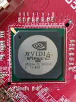
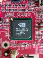
The AMD751 chipset is hardcoded to SysPushPull=0 which is the recommended setting for Slot-A, this chipset probably wasn't meant to operate together with PushPull drivers. AMD never officially offered this chipset for their Socket-A platform. It is possible though, the Gigabyte 7IXE4 used this chipset in combination with Socket-A and PushPull drivers. Gigabyte had to add a seperate microcontroller to the motherboard to manipulate the ROMSIP such that SysPushPull is configured as 1 for enabling the drivers. They probably had a whole lot of AMD chipsets laying around that they had to get rid of in this manner.

VIA's approach was different. The KX133 chipset was released in early 2000, which was right between the release of the AMD751 chipset (June 1999) and the release of the newer Thunderbird Socket-A cpu's. (June 2000) Because of this, the chipset was designed for both Slot-A and Socket-A in order to prevent a short lifecycle. The KX133 chipset was a Slot-A optimized version of what would later become the KT133 chipset, proof for this can be found in the KX133 revision guide:
"Removed “Socket-462” from description (chip is optimized for Slot-A) Updated VIA Logo to “Delivering Value” format"
The chipset was aimed at the newer Thunderbird cpu's that ran at higher bus speeds (133MHz instead of 100MHz) and used the PushPull driver interface. Thus the SysPushPull parameter is configured to 1 by default in this chipset. This value can be adjusted through a strapping pin by using a pull-up resistor on one of the adressing pins for the SD-RAM memory interface.

And now comes the part where shit hits the fan. A critical error was made on most of the KX133 boards; they didn't configure the state of the strapping pin for the SysPushPull parameter. (confirmed that on my Epox 7KXA board) With the introduction of the Thunderbird core, the SysPushPull parameter became relevant and a choice had to be made. Would the newer Slot-A cpu's keep using the open-drain interface for compatibility with the aging AMD chipset or would they switch to the PushPull interface for compatibility with the newer VIA chipset. AMD decided to keep using the Open-Drain interface on the Slot-A platform because all the AMD based boards that have been sold till that point were hardcoded for Open-Drain operation. They left VIA out in the cold here. :shot: This was especially painful since they were going through a lot of trouble with Intel for making an AMD chipset. (These were the evil days of Intel)

Many VIA boards were trying to run the newer Athlons in PushPull mode which resulted in instability since the pull-up resistors for the Open-Drain interface were interfering with the PushPull drivers. These resistors couldn't be removed as they were integrated into the CPU cartridge. I found an old article that also points in this direction:

As a result of this dumpster fire, AMD probably didn't allow the release of a Slotket adapter. They wanted to end the support for the Slot-A platform ASAP as a means of damage control for their relations with VIA. :wut: This is probably also why the Thunderbird Slot-A cpu's were initially OEM only and made in small numbers.

I do ask myself if the Asus K7V-T was a revision of the K7V to run in open-drain mode. This post got wayyy longer than anticipated.
 
Zuletzt bearbeitet:
The adapter is now officially in production, all production files have been verified and modified where needed. :d 
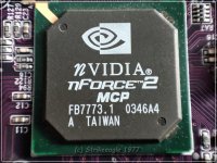
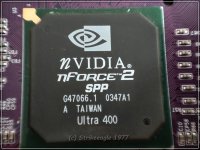
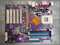
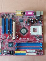
I also managed to find two more Slot A boards for testing:
- Biostar M7MKE (VIA KX133)
- Gigabyte 7IXE (AMD751)

The Gigabyte board is particularly interesting because it is the Slot A board that the 7IXE4 Socket A board is based on. It seems like crossflashing the bioses between these boards won't be a problem which is nice because i found a (working) modded bios for the 7IXE4 that has CPU support for Palomino, Thoroughbred and Barton. It would be interesting to try this bios on the 7IXE Slot A board and see if it would run with a Barton CPU. If the adapter actually works of course...
 
Hardwareluxx setzt keine externen Werbe- und Tracking-Cookies ein. Auf unserer Webseite finden Sie nur noch Cookies nach berechtigtem Interesse (Art. 6 Abs. 1 Satz 1 lit. f DSGVO) oder eigene funktionelle Cookies. Durch die Nutzung unserer Webseite erklären Sie sich damit einverstanden, dass wir diese Cookies setzen. Mehr Informationen und Möglichkeiten zur Einstellung unserer Cookies finden Sie in unserer Datenschutzerklärung.


Zurück
Oben Unten refresh