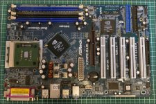
[Sammelthread] AMD K7 - Sockel A (462)

Sad news in my opinion. :(
I guess you tried the Socket A CPUs with the internal romsips with the Gigabyte board? I wonder how AMD managed the Slot A Thunderbirds to run on a non push-pull board. Do the CPU PCB have something to manipulate the SIP stream?

The FERR pin also isn't driven when using the adapter.
What does this pin do? I was not able to understand the datasheet. AMD mentions revisions though.

1685643926663.png


My final straw is manipulating the ROMSIP transfer in order to enable the PushPull drivers, but this will be a challenge.
good luck!
 
Wenn Du diese Anzeige nicht sehen willst, registriere Dich und/oder logge Dich ein.
Sad news in my opinion. :(
I guess you tried the Socket A CPUs with the internal romsips with the Gigabyte board? I wonder how AMD managed the Slot A Thunderbirds to run on a non push-pull board. Do the CPU PCB have something to manipulate the SIP stream?


What does this pin do? I was not able to understand the datasheet. AMD mentions revisions though.

Anhang anzeigen 892201


good luck!
I tried the internal romsip on the Socket-A Gigabyte board and it seems to behave exactly like the adapter. Nothing happens.... The Slot-A Thunderbird sillicon should be the same but it also uses the older BGA Slot-A package. I don't know how AMD managed to make it work in open-drain mode... These AMD cpu's do have a debugging/engineering interface that might have access to some additional registers that are needed to make the open-drain interface functional.

I did some research on those revisions a couple of days ago to debug the FERR signal but these revisions seem to be the last letter on the Slot-A cartridge identification code. Since all Slot-A motherboards don't mention specific revision support, i think there already is some kind of onboard circuit that takes care of these differences. I did change the FERR signal state by using a low resistance resistor but that didn't change anything in the behaviour, just to double check.

The important bits of the ROMSIP are hardcoded into the chipset indeed so it's very difficult to change this. The only way to modify the ROMSIP on the AMD chipset is to put it into Debug mode and attach an external EEPROM chip. But there isn't any documentation about how the chipset reads the memory and more importantly, this requires the usage of additional pins under the northbridge that are virtually impossible to reach once a motherboard is assembled.

The only way to change the ROMSIP will be to intercept the signal and replace it with another signal. The replacement signal must be skew-aligned to the CPU PLL clock signal though, and i hope that a delay in the signal of 2~3 clocks isn't breaking the protocol. It seems like everything is relatively loosely timed around the CONNECT signal so i hope my idea will work.
 
Zuletzt bearbeitet:
Does it make sense to check the SIP stream on a KX133 board? I mean we could try to find out if the VIA chip starts to use push-pull with a thunderbird. Or are my thoughts wrong?
Maybe the VIA chipset could help?
 
Out of curiosity i've checked the KT133 and KX133 datasheets. VIA doesn't even mention push-pull or open-drain anywhere. So either this is hardcoded or they switch it without any user-selectable option.
 
Well, i've received the Raspberry Pi Pico's but i don't think i can sync them (reliable) to the clock signal of the CPU which will mess up the timing of the SIP transfer. My next option will be the use of a CPLD (a simple form of an FPGA) but this is something that will take some time. Progress will still be made but from now on the daily updates will probably disappear... :shake:
 
Stock clock of the pico is 133Mhz, right? I assume that you'd need to at least overclock it heavily to get the I/O pins synced at 100Mhz... I read that it may run at up to 270MHz, that may come in handy when syncing to 100Mhz bus speed.
 
Stock clock of the pico is 133Mhz, right? I assume that you'd need to at least overclock it heavily to get the I/O pins synced at 100Mhz... I read that it may run at up to 270MHz, that may come in handy when syncing to 100Mhz bus speed.
Yeah that's correct. My plan was to overclock it to ~400MHz, this would give a maximum sync error of 1/4 clock cycle, unfortunately even the most simple programs need 2 to 3 clock cycles to read the input pin, forward it to the output pin and loop back to reading the input pin. This gives an actual sample rate of 133/200MHz which is still far too slow.

I'm currently looking at a Xilinx (AMD) XC2C64 CPLD which is a simpler variant of an FPGA. This chip got some nice features such as being able to be driven from the clock output of the CPU, making it far easier to skew align the data signal to the CPU clock signal. It can also run at relatively high frequencies, overclocking the bus speed to 110MHz+ should be no problem if stability allows for it. The input/output/threshold voltage of the IO pins is also variable and can be coupled to the Vcore voltage. So this chip should work with a Vcore ranging from 1.5~2.5v+, thus keeping all overclocking capabilities.

Unfortunately there aren't many plug&play boards for this chip, so i'll have to place an order on AliExpress which can take a while to arrive. Apart from that i will need to learn how these CPLD's work and how they have to be programmed. Apart from that i have to finish my electrical engineering study in the next months and prepare my Volvo 240 oldtimer for a vacation trip to the south of France. It needs an overhaul of the front suspension and the wiring of the custom ECU needs to be completely overhauled, i'll probably even make a simple 2 layer PCB for it as a distribution block for all the wiring. The ECU also still needs a good tune for both Petrol and Propane fuel. Actual progress on the adapter will probably be made again at the end of July / start of August...

There is a positive side on this story though. If i'm able to make it work i could probably produce a stand-alone device with the CPLD chip for injecting custom ROMSIPS... :d This ability could open a whole new box of pandora for hardware modding, not just for the AMD Slot/Socket A platform. Custom Intel Slotkets are also somewhere on my to-do list.
 
I got a bit carried away reading your post. Imagine you can make the sip injection work… you could even reimplement the whole cpu connect/disconnect cycle. Now imagine it’s possible to implement multiplier switching on nforce for superlocked CPUs…

I believe an Intel slotket which is Tualatin compatible and has all necessary mods would be of interest for the community. Especially when it’s moderately priced. This would make the modded tualatin obsolete and you could use any cpu on a slot board.

prepare my Volvo 240 oldtimer
Nice, another car guy. I own a (quite new) Volkswagen Passat B4 myself, sadly it’s been sitting in the garage and gathering dust for quite too long.
 
Zuletzt bearbeitet:
Nice, another car guy. I own a (quite new) Volkswagen Passat B4 myself, sadly it’s been sitting in the garage and gathering dust for quite too long.

And you might have thought he just made some mods for Socket A and Slot A... It is easily faster then my 3 series.
 
Zuletzt bearbeitet:
Mahlzeit!
Ich teste zur Zeit an meinem MSI K7T PRO (VIA KT133), bzw. an meinem MSI K7T Turbo2 (VIA KT133A) herum. Beide boards laufen noch mit SD RAM. Mir ist aufgefallen wie sehr der SDRAM den Sockel A limitert. Ich wollte das hier mal teilen. Villeicht ist das dem einen oder Anderen interessant. Mir war das vorher nicht so klar.
Parallel habe ich auch hier an den PCI registern verstellt um etwas mehr Leistung zu bekommen.

Testsystem:
Code:
MSI K7T PRO / VIA KT133 Chipset
AMD XP 3000+ @ 13x100MHz
2x128MB Micron 7B-G SDRAM @2-2-2-5
Radeon 9100 @ default

default
1:1 ratio
FSB : RAM
100MHz : 100MHz
tuned
1:1 ratio
FSB : RAM
100MHz : 100MHz
default
4:3 ratio
FSB : RAM
100MHz : 133MHz
tuned
4:3 ratio
FSB : RAM
100MHz : 133MHz
OC (+tuned)
1:1 ratio
FSB : RAM
115MHz : 115MHz
OC (+tuned)
4:3 ratio
FSB : RAM
115MHz : 153MHz
SuperPI 1M1m 36,859s1m 34,807s1m 30,610s1m 28,096s1m 22,278s1m 18,993s
Quake3A timedemo 001133,9fps136,2fps147,8fps149,7fps--
Unreal1 timedemo (640x480x16)107,34fps108,9fps115,07fps118,1fps--
AIDA memory READ788 MB/s786 MB/s1046 MB/s1050 MB/s907 MB/s1208 MB/s
AIDA memory WRITE630 MB/s789 MB/s835 MB/s1047 MB/s903 MB/s1208 MB/s
AIDA memory COPY694 MB/s780 MB/s925 MB/s1042 MB/s896 MB/s1200 MB/s
AIDA memory Latency219,4 ns219,2 ns198,8 ns198,8 ns190,5ns173 ns


Wie man sieht, ist der RAM Teiler bei 100MHz FSB auf 133MHz RAM Takt hier ein deutlicher Vorteil. Nicht nur in 2D, sondern genauso auch in 3D. Das entspricht in etwa 7% Leistung! Wenn ich mich recht erinnere, bringen höhere RAM Taktraten gegenüber dem FSB bei den späteren Chipsätzen mit DDR RAM deutlich weniger Leistung als hier mit SDRAM. Ich gehe davon aus, dass der SDRAM hier der größere Flaschenhals ist als der FSB. Kein Wunder, dass der KT266 Chipsatz mit DDR RAM deutlich zulegen konnte. Mit höherem FSB Takt sinkt scheinbar der RAM Takt Vorteil auf ca. 5%.

Die Tuning-Maßnahmen zeigen auch Wirkung. Hier gibt es auch ein kleines Plus. Es profitiert hier hauptsächlich der RAM Durchsatz bei Schreiben und Kopieren. Mit der Optimierung wird der RAM maximal ausgelastet.

Ich denke, die Optimierungen könnte man auch für den KX133 Chipsatz anwenden. Das wäre was für die SlotA Nutzer.

Eine Sache ist mir dann noch bei CPU-Z aufgefallen. Bei dem asynchronen FSB:RAM Takt addiert CPU-Z stupide die 33MHz dazu ohne dabei auf die FSB:RAM Teiler zu achten. :fresse: AIDA (und Everest) zeigt wohl den richtigen RAM Takt an. Also aufpassen! :d
 
Bei dem asynchronen FSB:RAM Takt addiert CPU-Z stupide die 33MHz dazu ohne dabei auf die FSB:RAM Teiler zu achten.
Das liegt wohl an VIA... Im Datenblatt steht bei den Ramteilern dabei +33Mhz, nicht 4:3. Ob das nun ein Irrtum im Datenblatt des kt133a ist wäre die Frage. Der Unterschied ist bei 115Mhz derart gering zwischen 4:3 und +33Mhz, das kann man wohl nur mit einem Oszi nachmessen.

Deine Ergebnisse wundern mich insofern nicht, da SDRAM die halbe Bandbreite des FSB hat. Klar verhungert der Athlon ggü DDR… Wie weit kannst du den FSB ziehen, damit der SDR ordentlich Takt bekommt? Ich tippe mit 200MHz+ 2-2-2 käme da richtig Leistung bei rum.

An der Stelle muss ich mich mal einlesen, ob der Pentium 3 auch so extrem von DDR profitiert hat. Gerade ein Tualatin bei 1.8ghz sollte nochmal einen Schub bekommen.
 
Zuletzt bearbeitet:
Das liegt wohl an VIA... Im Datenblatt steht bei den Ramteilern dabei +33Mhz, nicht 4:3. Ob das nun ein Irrtum im Datenblatt des kt133a ist wäre die Frage. Der Unterschied ist bei 115Mhz derart gering zwischen 4:3 und +33Mhz, das kann man wohl nur mit einem Oszi nachmessen.
Ich bin mir da auch nicht sicher. Im Bot haben die geschrieben, dass CPU-Z falsch ist. Ich habe auch gelesen, dass der PCI Takt addiert wird. Würde dann auch 115MHz+38MHz=153MHz ergeben. Bin mir also nicht sicher, was richtig ist. Der 4:3 Teiler macht in meinen Augen mehr Sinn. Klar, der Unterschied ist nicht so hoch. Dennoch...

Deine Ergebnisse wundern mich insofern nicht, da SDRAM die halbe Bandbreite des FSB hat. Klar verhungert der Athlon ggü DDR… Wie weit kannst du den FSB ziehen, damit der SDR ordentlich Takt bekommt? Ich tippe mit 200MHz+ 2-2-2 käme da richtig Leistung bei rum.
200MHz schaffe ich nicht. Der hier getestete KT133 schafft die 110MHz-115MHz FSB. Der KT133A schafft ca. 160MHz-170MHz in 1:1. Bei 133MHz FSB strap kann man leider nicht mit RAM Teiler schalten. Nur noch 1:1. So oder so, ich bin RAM Takt her bis ca. 170MHz limitiert. Muss aber noch verschiedene RAM Riegel testen.
Ich denke nicht, dass es SDRAM gibt, der 200MHz 2-2-2-5 schafft.😅
 
Bei 133MHz FSB strap kann man leider nicht mit RAM Teiler schalten.
Das ist ja blöd. Und mit dem 100er Strap kommst du vermutlich an FSB nicht weit...

Ich denke nicht, dass es SDRAM gibt, der 200MHz 2-2-2-5 schafft.😅

Najaaaa.... Qimonda FE-7 :d Oder Promos VDI7PC.
 
Najaaaa.... Qimonda FE-7 :d Oder Promos VDI7PC.
Terras Ergebnis kannte ich noch gar nicht. Ich habe gesehen, dass es Ergebnisse >210MHz gibt, waren aber meist auch mit deutlich mehr Spannung und mit CL3.

Den Vogons Thread kenne ich. Die guten Riegel sind sehr selten. :d Nicht unmöglich, aber selten. Ich werde sehen. Bei den KT133er boards lohnt sich das sammeln eigentlich nicht nicht. Die Intels können deutlich mehr, aber dafür fange ich mit P3 nicht an.
Ein paar Riegel habe ich hier und die werde ich mal auf Takt und timings testen. Vielleicht ergibt sich daraus ein Bild....

Das ist ja blöd. Und mit dem 100er Strap kommst du vermutlich an FSB nicht weit...
ab 125MHz bekomme ich einen freeze. Egal ob KT133 oder KT133A. Keine Ahnung. Unmöglich sollte das aber nicht sein. Werde noch testen müssen. Vielleicht liegt das an einer Einstellung? RAM?

edit:
166MHz / 2-2-2-5 bekomme ich aber hin! :d

edit:
 
Zuletzt bearbeitet:
Moin,

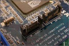
neueste Errungenschaft - leider etwas lädierter SATA Port,
nicht mein erstes MAl bei SATA, dennoch ist mir so etwas nie passiert bei SATA Ports

sry, aktuell nur schlechte Handybilder, ich reiche bessere noch nach.

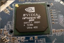
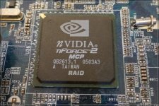
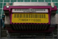
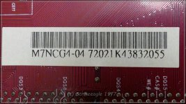
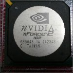
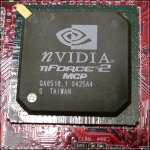
K7NF2-RAIDv1.042005/02A1SPP Ultra 4002005/03A3MCP RAIDblau--Strikeeagle1977--71M0X1110300
 

Anhänge

  • kl_P1200933.jpg
    kl_P1200933.jpg
    108,7 KB · Aufrufe: 55
  • kl_P1200934.jpg
    kl_P1200934.jpg
    120,5 KB · Aufrufe: 53
  • kl_P1200936.jpg
    kl_P1200936.jpg
    75,1 KB · Aufrufe: 56
  • kl_P1200937.jpg
    kl_P1200937.jpg
    109,4 KB · Aufrufe: 58
  • kl_P1200932.jpg
    kl_P1200932.jpg
    177 KB · Aufrufe: 59
Zuletzt bearbeitet:
Ich gebe das Board gerne weiter ... hab doch das Biostar, mit dem ich eigentlich glücklich bin. Das Board war nur Beifang, genauso wie die -ach du Schreck- die Quadro und der RAM ...
 
Der kleine kam die Tage an. Hat sich niemand für interessiert, da falsch eingestellt, also hab ich ihn genommen :fresse:

IMG_1882_luxx.jpg


IMG_1882_2_luxx.jpg


Bei 35°C Raumtemperatur unterm Dach gestern mal kurz mit 12x200 befeuert um zu schauen ob das geht und yes, das funktioniert. Auf mehr als 8M konnte ich mich wegen der Hitze aber nicht einlassen :fresse:
12,5x200 kommen zwar ins Windows, aber bei Last schmeißt SuperPi dann "Not exact in round".

Scheint also zumindest nicht graupig zu sein das Teil. Wird wenn es kühler ist mal weiter getestet.
 
Ja, 1,65V im Bios, ca. 1,61-1,63V unter Windows wenn Last drauf kommt. Aber wie gesagt, mit 12,5x200 war nur booten drin, keine Last, das geht nur mit 12x200 problemlos.
 
Glückwunsch! Manchmal muss man auch Finderglück haben. Selbes Stepping und Datum wie meiner aus post #8.718.
Ich denke mal, dass beide CPUs ähnlich takten werden.

Btw., hast du mal nachgemessen, wie weit das NF7 den Vdroop hat? Bei mir war es gemessen nicht so viel wie angezeigt.
Bei meinem älteren NF7 muss ich die Spannung meist höher stellen um ähnliche Taktraten zu erreicht. Das neuere NF7 mit bunten RAM Bänken hat das nicht.
 
Den hatte ich gesehen, aber wegen der recht frühen Woche liegen lassen. Sieht aber brauchbar aus, Glückwunsch!

Bei mir stapelt sich mittlerweile das Material, da verzichtet man gerne… einen noch größeren pile of shame brauche ich definitiv nicht :d da liegen mittlerweile schon das ECS und ein DFI Ultra-D drauf, muss reichen.

Erstmal ist das ECS dran, dann kommt das Ultra-D an die Reihe.
 
Zuletzt bearbeitet:

Anhänge

  • kl_P1200948.jpg
    kl_P1200948.jpg
    282,7 KB · Aufrufe: 67
  • kl_P1200950.jpg
    kl_P1200950.jpg
    117,8 KB · Aufrufe: 43
  • kl_P1200951.jpg
    kl_P1200951.jpg
    139,5 KB · Aufrufe: 48
  • kl_P1200952.jpg
    kl_P1200952.jpg
    180,4 KB · Aufrufe: 50
  • kl_P1200953.jpg
    kl_P1200953.jpg
    162,7 KB · Aufrufe: 43
I wanted to run some Socket A cpu's which are new in for a while now. Just when I wanted to turn on power to my 8RDA6+ I noticed the waterbath flowing fast on my motherboard...
Turns out the hose came lose. Maybe a payment for my lack of Socket A benching lately...
 
Oh no. I hope the board still works? It isn't a very common board...
 
Well I did not power it on and immediately got the water off, so I hope I saved it. I also blew hot air over it and now I let it dry up for at least 24 hours. That should do the trick.

Edit: Besides that I use the proper typer of water and additives.
 
I wanted to run some Socket A cpu's which are new in for a while now. Just when I wanted to turn on power to my 8RDA6+ I noticed the waterbath flowing fast on my motherboard...
Turns out the hose came lose. Maybe a payment for my lack of Socket A benching lately...
And it's dead...

Code 2b when using a PCI GFX card and F2 when using an AGP card.
 
I'd let it sit for some more days maybe. Usually they don't die because of that, heck I drown them for cleaning and not a single one didn't come back to life after getting rid of all the water. Maybe you still got water trapped beneath the chipset or something.
 
Hardwareluxx setzt keine externen Werbe- und Tracking-Cookies ein. Auf unserer Webseite finden Sie nur noch Cookies nach berechtigtem Interesse (Art. 6 Abs. 1 Satz 1 lit. f DSGVO) oder eigene funktionelle Cookies. Durch die Nutzung unserer Webseite erklären Sie sich damit einverstanden, dass wir diese Cookies setzen. Mehr Informationen und Möglichkeiten zur Einstellung unserer Cookies finden Sie in unserer Datenschutzerklärung.


Zurück
Oben Unten refresh