[Sammelthread] Intel DDR5 RAM OC Thread

Ah I see you want those screenshots, I do some runs for you.
Nono not for me , haha
Its imaginable.
But if you want to give voltage preset and say "its stable"

Haha, people like to see how temps are mid load.
1705881809677.png

Like with idle voltages , i dont know what to learn from it ~ you know :-)
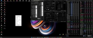
This screenshot never saw load. There is no y-cruncher bandwidth
There is no TM5 duration time. I dont know what to do with words.
I hope you understand.

Is it PSU OFF , reboot stable ?
Tm5 ~ attached
y-cruncher http://www.numberworld.org/y-cruncher/y-cruncher v0.8.3.9532.zip
ATC https://drive.google.com/file/d/1-PdgLkCf-5cA3b1kqO2CmFyhXtz-tiS3/view
 

Anhänge

  • TM5_0.12.3_1usmus25-CoolCMD.zip
    25 KB · Aufrufe: 58
Wenn Du diese Anzeige nicht sehen willst, registriere Dich und/oder logge Dich ein.
used trfc mini, if looks correct i will be satisfied for ram
[2024/01/21 21:33:23]
Ai Overclock Tuner [XMP Tweaked]
XMP [DDR5-7800 36-46-46-125-1.45V-1.45V]
BCLK Frequency [100.0000]
PCIE Frequency [100.0000]
Intel(R) Adaptive Boost Technology [Auto]
ASUS MultiCore Enhancement [Enabled – Remove All limits]
SVID Behavior [Auto]
BCLK Frequency : DRAM Frequency Ratio [Auto]
Memory Controller : DRAM Frequency Ratio [Auto]
DRAM Frequency [DDR5-7800MHz]
DIMM Flex [Disabled]
Performance Core Ratio [Sync All Cores]
ALL-Core Ratio Limit [51]
Performance Core0 Specific Ratio Limit [51]
Performance Core0 specific Voltage [Auto]
Performance Core1 Specific Ratio Limit [51]
Performance Core1 specific Voltage [Auto]
Performance Core2 Specific Ratio Limit [51]
Performance Core2 specific Voltage [Auto]
Performance Core3 Specific Ratio Limit [51]
Performance Core3 specific Voltage [Auto]
*Performance Core4 Specific Ratio Limit [51]
Performance Core4 specific Voltage [Auto]
*Performance Core5 Specific Ratio Limit [51]
Performance Core5 specific Voltage [Auto]
Performance Core6 Specific Ratio Limit [51]
Performance Core6 specific Voltage [Auto]
Performance Core7 Specific Ratio Limit [51]
Performance Core7 specific Voltage [Auto]
AVX2 [Auto]
AVX2 Ratio Offset to per-core Ratio Limit [User Specify]
AVX2 Ratio Offset [0]
AVX2 Voltage Guardband Scale Factor [User Specify]
AVX2 Voltage Guardband Scale Factor [0]
Maximus Tweak [Mode 1]
DRAM CAS# Latency [36]
DRAM RAS# to CAS# Delay Read [46]
DRAM RAS# to CAS# Delay Write [46]
DRAM RAS# PRE Time [46]
DRAM RAS# ACT Time [58]
DRAM Command Rate [2N]
DRAM RAS# to RAS# Delay L [8]
DRAM RAS# to RAS# Delay S [8]
DRAM REF Cycle Time 2 [512]
DRAM REF Cycle Time Same Bank [422]
DRAM Refresh Interval [32767]
DRAM WRITE Recovery Time [Auto]
DRAM READ to PRE Time [12]
DRAM FOUR ACT WIN Time [32]
DRAM WRITE to READ Delay L [15]
DRAM WRITE to READ Delay S [3]
DRAM CKE Minimum Pulse Width [20]
DRAM Write Latency [Auto]
Ctl0 dqvrefup [Auto]
Ctl0 dqvrefdn [Auto]
Ctl0 dqodtvrefup [Auto]
Ctl0 dqodtvrefdn [Auto]
Ctl1 cmdvrefup [Auto]
Ctl1 ctlvrefup [Auto]
Ctl1 clkvrefup [Auto]
Ctl1 ckecsvrefup [Auto]
Ctl2 cmdvrefdn [Auto]
Ctl2 ctlvrefdn [Auto]
Ctl2 clkvrefdn [Auto]
Read Equalization RxEq Start Sign [-]
Read Equalization RxEq Start [Auto]
Read Equalization RxEq Stop Sign [-]
Read Equalization RxEq Stop [Auto]
ODT_READ_DURATION [Auto]
ODT_READ_DELAY [Auto]
ODT_WRITE_DURATION [Auto]
ODT_WRITE_DELAY [Auto]
DQ RTT WR [Auto]
DQ RTT NOM RD [Auto]
DQ RTT NOM WR [Auto]
DQ RTT PARK [Auto]
DQ RTT PARK DQS [Auto]
GroupA CA ODT [Auto]
GroupA CS ODT [Auto]
GroupA CK ODT [Auto]
GroupB CA ODT [Auto]
GroupB CS ODT [Auto]
GroupB CK ODT [Auto]
Pull-up Output Driver Impedance [Auto]
Pull-Down Output Driver Impedance [Auto]
Round Trip Latency Init Value MC0 CHA [Auto]
Round Trip Latency Max Value MC0 CHA [Auto]
Round Trip Latency Offset Value Mode Sign MC0 CHA [-]
Round Trip Latency Offset Value MC0 CHA [Auto]
Round Trip Latency Init Value MC0 CHB [Auto]
Round Trip Latency Max Value MC0 CHB [Auto]
Round Trip Latency Offset Value Mode Sign MC0 CHB [-]
Round Trip Latency Offset Value MC0 CHB [Auto]
Round Trip Latency Init Value MC1 CHA [Auto]
Round Trip Latency Max Value MC1 CHA [Auto]
Round Trip Latency Offset Value Mode Sign MC1 CHA [-]
Round Trip Latency Offset Value MC1 CHA [Auto]
Round Trip Latency Init Value MC1 CHB [Auto]
Round Trip Latency Max Value MC1 CHB [Auto]
Round Trip Latency Offset Value Mode Sign MC1 CHB [-]
Round Trip Latency Offset Value MC1 CHB [Auto]
Round Trip Latency MC0 CHA R0 [Auto]
Round Trip Latency MC0 CHA R1 [Auto]
Round Trip Latency MC0 CHA R2 [Auto]
Round Trip Latency MC0 CHA R3 [Auto]
Round Trip Latency MC0 CHA R4 [Auto]
Round Trip Latency MC0 CHA R5 [Auto]
Round Trip Latency MC0 CHA R6 [Auto]
Round Trip Latency MC0 CHA R7 [Auto]
Round Trip Latency MC0 CHB R0 [Auto]
Round Trip Latency MC0 CHB R1 [Auto]
Round Trip Latency MC0 CHB R2 [Auto]
Round Trip Latency MC0 CHB R3 [Auto]
Round Trip Latency MC0 CHB R4 [Auto]
Round Trip Latency MC0 CHB R5 [Auto]
Round Trip Latency MC0 CHB R6 [Auto]
Round Trip Latency MC0 CHB R7 [Auto]
Round Trip Latency MC1 CHA R0 [Auto]
Round Trip Latency MC1 CHA R1 [Auto]
Round Trip Latency MC1 CHA R2 [Auto]
Round Trip Latency MC1 CHA R3 [Auto]
Round Trip Latency MC1 CHA R4 [Auto]
Round Trip Latency MC1 CHA R5 [Auto]
Round Trip Latency MC1 CHA R6 [Auto]
Round Trip Latency MC1 CHA R7 [Auto]
Round Trip Latency MC1 CHB R0 [Auto]
Round Trip Latency MC1 CHB R1 [Auto]
Round Trip Latency MC1 CHB R2 [Auto]
Round Trip Latency MC1 CHB R3 [Auto]
Round Trip Latency MC1 CHB R4 [Auto]
Round Trip Latency MC1 CHB R5 [Auto]
Round Trip Latency MC1 CHB R6 [Auto]
Round Trip Latency MC1 CHB R7 [Auto]
Early Command Training [Auto]
SenseAmp Offset Training [Auto]
Early ReadMPR Timing Centering 2D [Auto]
Read MPR Training [Auto]
Receive Enable Training [Auto]
Jedec Write Leveling [Auto]
Early Write Time Centering 2D [Auto]
Early Read Time Centering 2D [Auto]
Write Timing Centering 1D [Auto]
Write Voltage Centering 1D [Auto]
Read Timing Centering 1D [Auto]
Read Timing Centering with JR [Auto]
Dimm ODT Training* [Auto]
Max RTT_WR [ODT Off]
DIMM RON Training* [Auto]
Write Drive Strength/Equalization 2D* [Auto]
Write Slew Rate Training* [Auto]
Read ODT Training* [Auto]
Comp Optimization Training [Auto]
Read Equalization Training* [Auto]
Read Amplifier Training* [Auto]
Write Timing Centering 2D [Auto]
Read Timing Centering 2D [Auto]
Command Voltage Centering [Auto]
Early Command Voltage Centering [Auto]
Write Voltage Centering 2D [Auto]
Read Voltage Centering 2D [Auto]
Late Command Training [Enabled]
Round Trip Latency [Auto]
Turn Around Timing Training [Auto]
CMD CTL CLK Slew Rate [Auto]
CMD/CTL DS & E 2D [Auto]
Read Voltage Centering 1D [Auto]
TxDqTCO Comp Training* [Auto]
ClkTCO Comp Training* [Auto]
TxDqsTCO Comp Training* [Auto]
VccDLL Bypass Training [Auto]
CMD/CTL Drive Strength Up/Dn 2D [Auto]
DIMM CA ODT Training [Auto]
PanicVttDnLp Training* [Auto]
Read Vref Decap Training* [Auto]
Vddq Training [Auto]
Duty Cycle Correction Training [Auto]
Periodic DCC [Auto]
Rank Margin Tool Per Bit [Auto]
DIMM DFE Training [Auto]
EARLY DIMM DFE Training [Auto]
Tx Dqs Dcc Training [Auto]
DRAM DCA Training [Auto]
Write Driver Strength Training [Auto]
Rank Margin Tool [Auto]
Memory Test [Auto]
DIMM SPD Alias Test [Auto]
Receive Enable Centering 1D [Auto]
Retrain Margin Check [Auto]
Write Drive Strength Up/Dn independently [Auto]
LPDDR DqDqs Re-Training [Auto]
Margin Check Limit [Disabled]
tRDRD_sg_Training [Auto]
tRDRD_sg_Runtime [16]
tRDRD_dg_Training [Auto]
tRDRD_dg_Runtime [8]
tRDWR_sg [19]
tRDWR_dg [19]
tWRWR_sg [16]
tWRWR_dg [8]
tWRRD_sg [Auto]
tWRRD_dg [Auto]
tRDRD_dr [1]
tRDRD_dd [1]
tRDWR_dr [1]
tRDWR_dd [1]
tWRWR_dr [1]
tWRWR_dd [1]
tWRRD_dr [1]
tWRRD_dd [1]
tRPRE [Auto]
tWPRE [Auto]
tWPOST [Auto]
tWRPRE [Auto]
tPRPDEN [2]
tRDPDEN [Auto]
tWRPDEN [66]
tCPDED [20]
tREFIX9 [Auto]
Ref Interval [Auto]
tXPDLL [Auto]
tXP [29]
tPPD [2]
tCCD_L_tDLLK [Auto]
tZQCAL [Auto]
tZQCS [Auto]
OREF_RI [Auto]
Refresh Watermarks [High]
Refresh Hp Wm [Auto]
Refresh Panic Wm [Auto]
Refresh Abr Release [Auto]
tXSDLL [Auto]
tZQOPER [Auto]
tMOD [Auto]
CounttREFIWhileRefEn [Auto]
HPRefOnMRS [Auto]
SRX Ref Debits [Auto]
RAISE BLK WAIT [Auto]
Ref Stagger En [Auto]
Ref Stagger Mode [Auto]
Disable Stolen Refresh [Auto]
En Ref Type Display [Auto]
Trefipulse Stagger Disable [Auto]
tRPab ext [Auto]
derating ext [Auto]
Allow 2cyc B2B LPDDR [Auto]
tCSH [Auto]
tCSL [Auto]
powerdown Enable [Auto]
idle length [Auto]
raise cke after exit latency [Auto]
powerdown latency [Auto]
powerdown length [Auto]
selfrefresh latency [Auto]
selfrefresh length [Auto]
ckevalid length [Auto]
ckevalid enable [Auto]
idle enable [Auto]
selfrefresh enable [Auto]
Address mirror [Auto]
no gear4 param divide [Auto]
x8 device [Auto]
no gear2 param divide [Auto]
ddr 1dpc split ranks on subch [Auto]
write0 enable [Auto]
MultiCycCmd [Auto]
WCKDiffLowInIdle [Auto]
PBR Disable [Auto]
PBR OOO Dis [Auto]
PBR Disable on hot [Auto]
PBR Exit on Idle Cnt [Auto]
tXSR [550]
Dec tCWL [Auto]
Add tCWL [Auto]
Add 1Qclk delay [Auto]
MRC Fast Boot [Disabled]
MCH Full Check [Enabled]
Mem Over Clock Fail Count [Auto]
Training Profile [Auto]
RxDfe [Auto]
Mrc Training Loop Count [Auto]
DRAM CLK Period [Auto]
Dll_bwsel [Auto]
Controller 0, Channel 0 Control [Enabled]
Controller 0, Channel 1 Control [Enabled]
Controller 1, Channel 0 Control [Enabled]
Controller 1, Channel 1 Control [Enabled]
MC_Vref0 [Auto]
MC_Vref1 [Auto]
MC_Vref2 [Auto]
Fine Granularity Refresh mode [Enabled]
SDRAM Density Per Die [Auto]
SDRAM Banks Per Bank Group [Auto]
SDRAM Bank Groups [Auto]
Dynamic Memory Boost [Disabled]
Realtime Memory Frequency [Disabled]
SA GV [Disabled]
Voltage Monitor [Die Sense]
VRM Initialization Check [Enabled]
CPU Input Voltage Load-line Calibration [Auto]
CPU Load-line Calibration [Level 5]
Synch ACDC Loadline with VRM Loadline [Disabled]
CPU Current Capability [Auto]
CPU Current Reporting [Auto]
Core Voltage Suspension [Auto]
CPU VRM Switching Frequency [Auto]
VRM Spread Spectrum [Auto]
CPU Power Duty Control [Extreme]
CPU Power Phase Control [Extreme]
CPU Power Thermal Control [125]
CPU Core/Cache Boot Voltage [Auto]
CPU Input Boot Voltage [Auto]
PLL Termination Boot Voltage [Auto]
CPU Standby Boot Voltage [Auto]
Memory Controller Boot Voltage [Auto]
CPU Core Auto Voltage Cap [Auto]
CPU Input Auto Voltage Cap [Auto]
Memory Controller Auto Voltage Cap [Auto]
Maximum CPU Core Temperature [Auto]
Fast Throttle Threshold [Auto]
Package Temperature Threshold [Auto]
Regulate Frequency by above Threshold [Auto]
IVR Transmitter VDDQ ICCMAX [Auto]
Unlimited ICCMAX [Auto]
CPU Core/Cache Current Limit Max. [Auto]
Long Duration Package Power Limit [Auto]
Package Power Time Window [Auto]
Short Duration Package Power Limit [Auto]
Dual Tau Boost [Disabled]
IA AC Load Line [Auto]
IA DC Load Line [Auto]
IA CEP Enable [Disabled]
SA CEP Enable [Disabled]
IA SoC Iccmax Reactive Protector [Auto]
Inverse Temperature Dependency Throttle [Auto]
IA VR Voltage Limit [Auto]
CPU SVID Support [Auto]
Cache Dynamic OC Switcher [Auto]
TVB Voltage Optimizations [Disabled]
Enhanced TVB [Auto]
Overclocking TVB [Auto]
Overclocking TVB Global Temperature Offset Sign [+]
Overclocking TVB Global Temperature Offset Value [Auto]
Offset Mode Sign 1 [+]
V/F Point 1 Offset [Auto]
Offset Mode Sign 2 [+]
V/F Point 2 Offset [Auto]
Offset Mode Sign 3 [+]
V/F Point 3 Offset [Auto]
Offset Mode Sign 4 [+]
V/F Point 4 Offset [Auto]
Offset Mode Sign 5 [+]
V/F Point 5 Offset [Auto]
Offset Mode Sign 6 [+]
V/F Point 6 Offset [Auto]
Offset Mode Sign 7 [+]
V/F Point 7 Offset [Auto]
Offset Mode Sign 8 [+]
V/F Point 8 Offset [Auto]
Offset Mode Sign 9 [+]
V/F Point 9 Offset [Auto]
Offset Mode Sign 10 [+]
V/F Point 10 Offset [Auto]
Offset Mode Sign 11 [+]
V/F Point 11 Offset [Auto]
Initial BCLK Frequency [Auto]
Runtime BCLK OC [Auto]
BCLK Amplitude [Auto]
BCLK Slew Rate [Auto]
BCLK Spread Spectrum [Auto]
Initial PCIE Frequency [Auto]
PCIE/DMI Amplitude [Auto]
PCIE/DMI Slew Rate [Auto]
PCIE/DMI Spread Spectrum [Auto]
Cold Boot PCIE Frequency [Auto]
Realtime Memory Timing [Enabled]
SPD Write Disable [TRUE]
PVD Ratio Threshold [Auto]
SA PLL Frequency Override [Auto]
BCLK TSC HW Fixup [Enabled]
Core Ratio Extension Mode [Disabled]
FLL OC mode [Auto]
UnderVolt Protection [Disabled]
Switch Microcode [Current Microcode]
Core PLL Voltage [Auto]
GT PLL Voltage [Auto]
Ring PLL Voltage [Auto]
System Agent PLL Voltage [Auto]
Memory Controller PLL Voltage [Auto]
CPU 1.8V Small Rail [Auto]
PLL Termination Voltage [Auto]
CPU Standby Voltage [Auto]
PCH 1.05V Voltage [Auto]
PCH 0.82V Voltage [Auto]
CPU Input Voltage Reset Voltage [Auto]
Eventual CPU Input Voltage [Auto]
Eventual Memory Controller Voltage [Auto]
Package Temperature Threshold [Auto]
Regulate Frequency by above Threshold [Auto]
Cooler Efficiency Customize [Keep Training]
Cooler Re-evaluation Algorithm [Normal]
Optimism Scale [100]
Ring Down Bin [Disabled]
Min. CPU Cache Ratio [45]
Max. CPU Cache Ratio [45]
BCLK Aware Adaptive Voltage [Auto]
Actual VRM Core Voltage [Manual Mode]
- CPU Core Voltage Override [1.20000]
Global Core SVID Voltage [Auto]
Cache SVID Voltage [Auto]
CPU System Agent Voltage [Auto]
CPU Input Voltage [Auto]
High DRAM Voltage Mode [Enabled]
DRAM VDD Voltage [1.45000]
DRAM VDDQ Voltage [1.45000]
IVR Transmitter VDDQ Voltage [Auto]
Memory Controller Voltage [Auto]
MC Voltage Calculation Voltage Base [Auto]
VDD Calculation Voltage Base [Auto]
PMIC Voltages [Sync All PMICs]
SPD HUB VLDO (1.8V) [Auto]
SPD HUB VDDIO (1.0V) [Auto]
DRAM VDD Voltage [1.45000]
DRAM VDDQ Voltage [1.45000]
DRAM VPP Voltage [Auto]
DRAM VDD Switching Frequency [Auto]
DRAM VDDQ Switching Frequency [Auto]
DRAM VPP Switching Frequency [Auto]
DRAM Current Capability [Auto]
PCI Express Native Power Management [Disabled]
DMI Link ASPM Control [Disabled]
ASPM [Disabled]
L1 Substates [Disabled]
DMI ASPM [Disabled]
DMI Gen3 ASPM [Disabled]
PEG - ASPM [Disabled]
PCI Express Clock Gating [Disabled]
Hardware Prefetcher [Enabled]
Adjacent Cache Line Prefetch [Enabled]
Intel (VMX) Virtualization Technology [Disabled]
Per P-Core Control [Disabled]
Per E-Core Control [Disabled]
Active Performance Cores [All]
Active Efficient Cores [0]
Hyper-Threading [Disabled]
Boot performance mode [Auto]
Intel(R) SpeedStep(tm) [Enabled]
Intel(R) Speed Shift Technology [Enabled]
Intel(R) Turbo Boost Max Technology 3.0 [Enabled]
Turbo Mode [Enabled]
Acoustic Noise Mitigation [Disabled]
CPU C-states [Disabled]
Thermal Monitor [Enabled]
Dual Tau Boost [Disabled]
VT-d [Disabled]
Memory Remap [Enabled]
Enable VMD controller [Enabled]
Map PCIE Storage under VMD [Disabled]
M.2_2 Link Speed [Auto]
PCIEX16(G5)_1 Link Speed [Auto]
M.2_1 Link Speed [Auto]
PCIEX4(G4)_1 Link Speed [Auto]
PCIEX4(G4)_2 Link Speed [Auto]
M.2_3 Link Speed [Auto]
DIMM.2_1 Link Speed [Auto]
DIMM.2_2 Link Speed [Auto]
SATA Controller(s) [Disabled]
PTT [Enable]
Intel(R) Dynamic Tuning Technology [Disabled]
PCIE Tunneling over USB4 [Enabled]
Discrete Thunderbolt(TM) Support [Disabled]
Security Device Support [Enable]
SHA256 PCR Bank [Enabled]
Pending operation [None]
Platform Hierarchy [Enabled]
Storage Hierarchy [Enabled]
Endorsement Hierarchy [Enabled]
Physical Presence Spec Version [1.3]
Disable Block Sid [Disabled]
Password protection of Runtime Variables [Disable]
Above 4G Decoding [Enabled]
Resize BAR Support [Enabled]
SR-IOV Support [Disabled]
Legacy USB Support [Disabled]
XHCI Hand-off [Disabled]
U10G_1 [Enabled]
U5G_E5 [Enabled]
U5G_E6 [Enabled]
U5G_E7 [Enabled]
U5G_E8 [Enabled]
U20G_C3 [Enabled]
U10G_5 [Enabled]
U10G_6 [Enabled]
U10G_7 [Enabled]
U10G_8 [Enabled]
U20G_C9 [Enabled]
USB11 [Enabled]
USB12 [Enabled]
U32G1_E1 [Enabled]
U32G1_E2 [Enabled]
U32G1_E3 [Enabled]
U32G1_E4 [Enabled]
Network Stack [Disabled]
Device [N/A]
Restore AC Power Loss [Power Off]
Max Power Saving [Disabled]
ErP Ready [Disabled]
Power On By PCI-E [Disabled]
Power On By RTC [Disabled]
USB Audio [Enabled]
Intel LAN [Enabled]
USB power delivery in Soft Off state (S5) [Enabled]
Wi-Fi Controller [Disabled]
Bluetooth Controller [Disabled]
When system is in working state [Stealth Mode]
M.2_3 Configuration [Auto]
CPU PCIE Configuration Mode [Auto]
ASMedia USB 3.2 Controller_U5G_E12 [Enabled]
ASMedia USB 3.2 Controller_U5G_E34 [Enabled]
GNA Device [Disabled]
Alteration Mode Switch [PCIE Link Speed]
CPU Temperature [Monitor]
CPU Package Temperature [Monitor]
MotherBoard Temperature [Monitor]
VRM Temperature [Monitor]
Chipset Temperature [Monitor]
T_Sensor Temperature [Monitor]
DIMM.2 Sensor 1 Temperature [Monitor]
DIMM.2 Sensor 2 Temperature [Monitor]
Water In T Sensor Temperature [Monitor]
Water Out T Sensor Temperature [Monitor]
DIMM Thermistor Temperature [Monitor]
DIMM A1 Temperature [Monitor]
DIMM B1 Temperature [Monitor]
CPU Fan Speed [Monitor]
CPU Optional Fan Speed [Monitor]
Chassis Fan 1 Speed [Monitor]
Chassis Fan 2 Speed [Monitor]
Extra Flow Fan Speed [Monitor]
Water Pump+ Speed [Monitor]
AIO Pump Speed [Monitor]
Flow Rate [Monitor]
CPU Core Voltage [Monitor]
12V Voltage [Monitor]
5V Voltage [Monitor]
3.3V Voltage [Monitor]
Memory Controller Voltage [Monitor]
CPU Fan Q-Fan Control [Auto Detect]
CPU Fan Profile [Turbo]
CPU Fan Q-Fan Source [CPU]
CPU Fan Step Up [Level 2]
CPU Fan Step Down [Level 2]
CPU Fan Speed Low Limit [200 RPM]
Chassis Fan 1 Q-Fan Control [DC Mode]
Chassis Fan 1 Profile [Full Speed]
Chassis Fan 2 Q-Fan Control [Auto Detect]
Chassis Fan 2 Profile [Standard]
Chassis Fan 2 Q-Fan Source [CPU]
Chassis Fan 2 Step Up [Level 0]
Chassis Fan 2 Step Down [Level 0]
Chassis Fan 2 Speed Low Limit [200 RPM]
Extra Flow Fan Q-Fan Control [Auto Detect]
Extra Flow Fan Profile [Standard]
Extra Flow Fan Q-Fan Source [DIMM Thermistor]
Extra Flow Fan Step Up [Level 0]
Extra Flow Fan Step Down [Level 0]
Extra Flow Fan Speed Low Limit [Ignore]
Water Pump+ Q-Fan Control [Auto Detect]
Water Pump+ Profile [Full Speed]
AIO Pump Q-Fan Control [Auto Detect]
AIO Pump Profile [Full Speed]
CPU Temperature LED Switch [Enabled]
Launch CSM [Disabled]
OS Type [Windows UEFI mode]
Secure Boot Mode [Standard]
Fast Boot [Disabled]
Boot Logo Display [Auto]
POST Delay Time [3 sec]
Bootup NumLock State [On]
Wait For 'F1' If Error [Enabled]
Option ROM Messages [Force BIOS]
Interrupt 19 Capture [Disabled]
AMI Native NVMe Driver Support [Enabled]
Setup Mode [Advanced Mode]
Boot Sector (MBR/GPT) Recovery Policy [Local User Control]
Next Boot Recovery Action [Skip]
BIOS Image Rollback Support [Enabled]
Publish HII Resources [Enabled]
Flexkey [Reset]
Setup Animator [Disabled]
Load from Profile [1]
Profile Name []
Save to Profile [1]
DIMM Slot Number [DIMM_A1]
Hotkey F3 [Boot to ASUS EZ Flash 3]
Hotkey F4 [Boot from UEFI USB]
Download & Install ARMOURY CRATE app [Enabled]
Download & Install MyASUS service & app [Disabled]
 
Nono not for me , haha
Its imaginable.
But if you want to give voltage preset and say "its stable"

Haha, people like to see how temps are mid load.
Anhang anzeigen 962434
Like with idle voltages , i dont know what to learn from it ~ you know :-)
This screenshot never saw load. There is no y-cruncher bandwidth
There is no TM5 duration time. I dont know what to do with words.
I hope you understand.

Is it PSU OFF , reboot stable ?
Tm5 ~ attached
y-cruncher http://www.numberworld.org/y-cruncher/y-cruncher v0.8.3.9532.zip
ATC https://drive.google.com/file/d/1-PdgLkCf-5cA3b1kqO2CmFyhXtz-tiS3/view
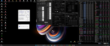
I see you man, no worries, is this better? :d

Yes it is cold boot stable and has no issues restarting.
 

Anhänge

  • Näyttökuva 2024-01-22 023347.png
    Näyttökuva 2024-01-22 023347.png
    179,4 KB · Aufrufe: 87
I see you man, no worries, is this better? :d

Yes it is cold boot stable and has no issues restarting.
Noo, this doesnt mean stability. What do you meaan. Please use what i linked

Uhhh , i mean ~ sure :giggle:
Thank youu !

Good memory cooling !
Do you want to try if 512 RFC (~124ns) will still keep long term stability up ?
Next step up is 544 RFC.

Minimum testing duration is usually 90min, for every piece of hardware.
Laws of physics and stuff~

EDIT:
Thermal equilibrium on fluid can be reached 10-15min in
Thermal equilibrium on cooling to room, usually happens near 45min
But duration of first noise based issues on longterm current ~ is 90min as a good goal.
For some over 120min, but it really depends what sort of autocorrection and guardbanding is used.

Soo 90min for any sort of hardware, is a good idea to follow :-)(y)
For example on any sort of overclock, as you are at the mercy of good power-quality.
 
Zuletzt bearbeitet:
Noo, this doesnt mean stability. What do you meaan. Please use what i linked

Uhhh , i mean ~ sure :giggle:
Thank youu !

Good memory cooling !
Do you want to try if 512 RFC (~124ns) will still keep long term stability up ?
Next step up is 544 RFC.

Minimum testing duration is usually 90min, for every piece of hardware.
Laws of physics and stuff~
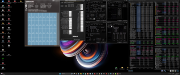
Sorry I started the run before I saw you reply.. but I've done longer runs. I wanted to show quickly that it wasn't all just talk :d

I can try RFC 512. Does RFCpb need to be touched?

Sticks are naked with somewhat direct airflow.
 

Anhänge

  • Näyttökuva 2024-01-22 033159.png
    Näyttökuva 2024-01-22 033159.png
    71,5 KB · Aufrufe: 86
I can try RFC 512. Does RFCpb need to be touched?
In this case yes
Its always lower than above value.

But i dont have magical values for it.
Its "usually" around 20-30ns faster.
But also usually they stay above 100-110ns

Up to capacity i guess.
JEDEC is no help, as qualifications are made at 1.1v
Same for REFI at 64ms charge retention time. (RET)
1705888750212.png

Example, but not target ~ just example what is the target @ 1.1/1.2v

448 could be just about right for RFCpb
I dont know about "steps of 26" rule, i read.
With "steps of 32" you can never go wrong.

tXSR for RFC512 is 552
For 554 RFC its 594
^ those are very tight and personal.
If we go by specifications, there is no need to touch those. But they give a bit perf.

If you want even more speed
WTRS = RRDS/2 ,, up to max same value
WTRL = RRDL*2. Up to *3
If you error it means a too short timing somewhere else
Or generally too low RRDL + extra reason.
^ no direct connection, but inside the box thinking, yes.


And after that is long time stable, just drop tRDWR_SG & DG
I would not recommend when chasing clock ~ but that also gives a chunk of perf.

I personally like to chase the clock rabbit, but i guess~~
Other timings can stay how they are, except CAS and RCD.
No need to scale other things down. Just causes transition conflicts.

Ah right, CWL = CAS-2 . Always !
 
Zuletzt bearbeitet:
In this case yes
Its always lower than above value.

But i dont have magical values for it.
Its "usually" around 20-30ns faster.
But also usually they stay above 100-110ns

Up to capacity i guess.
JEDEC is no help, as qualifications are made at 1.1v
Same for REFI at 64ms charge retention time. (RET)
Anhang anzeigen 962446
Example, but not target ~ just example what is the target @ 1.1/1.2v

448 could be just about right for RFCpb
I dont know about "steps of 26" rule, i read.
With "steps of 32" you can never go wrong.

tXSR for RFC512 is 552
For 554 RFC its 594
^ those are very tight and personal.
If we go by specifications, there is no need to touch those. But they give a bit perf.

If you want even more speed
WTRS = RRDS/2 ,, up to max same value
WTRL = RRDL*2. Up to *3
If you error it means a too short timing somewhere else
Or generally too low RRDL + extra reason.
^ no direct connection, but inside the box thinking, yes.


And after that is long time stable, just drop tRDWR_SG & DG
I would not recommend when chasing clock ~ but that also gives a chunk of perf.

I personally like to chase the clock rabbit, but i guess~~
Other timings can stay how they are, except CAS and RCD.
No need to scale other things down. Just causes transition conflicts.

Ah right, CWL = CAS-2 . Always !
Thanks very much man. I try these!
 
@ robonz ...geilstes 2 DIMM Board " EVGA DarK " :drool:

Echt schade das EVGA nicht mehr weiter macht in dem Bereich.

Jap, vor allem schade, dass die nicht mal eine letzte, aktuelle BIOS-Version rausgeholt haben für das Board…
 
8533 Mhz CL 34-47-46-32 mit 1.630v VDD
Autsch! 1,630V könnte ziemlich warm werden. Halten die das aus? Ich habe immer Angst, ich brutzel irgendwas durch. Darum überschreite ich manche Spannungen nicht, auch wenn es das Board zulässt.
Dein Aorus Tachyon, ist das das mit dem Z690 oder Z790? Ich selber komme gerade an die Grenzen eines Z690 Aorus Pro. Laut Gigabyte sollte da die Grenze eher 6200MT/s sein, meine letzten Versuche waren mit einem Kingston Renegade 7200MT/s Kit. Ich wollte erreichen, dass der Speicher 7600MT/s erreicht bzw. wenigstens 7400MT/s, leider sagten alle Versuche ab 7400MT/s nö im memtest.
Einzel schafft der Speicher ohne Murren und Zucken 7600MT/s und zeigt keine Fehler im memtest. Wenn aber beide Speicher drin sind, bleibt memtest nach ca. 20 Sekunden stehen.

Seit dem Bios Update vom Dezember schafft das Board jetzt aber die 7200MT/s mit angezogenen Timings. Mit dem Bios davor, war nicht mal das XMP Profil für die 7200MT/s stabil.

Bis auf die CPU Spannung, die ich für die Dauern von memtest auf "normal" lasse, stehen die Spannungen für alles Andere auf "auto". Es gibt ein paar gute Videos auf Youtube, wie man im Gigabyte Bios die Spannungen einstellen soll. Ich will nur lieber nicht daran herumfummeln und sinnlos irgendwo eine Spannung erhöhen und womöglich etwas durchbrennen.

Ich kann mir für die nächsten Jahre kein neues Board leisten. Bin ja schon froh, dass ich richtig geraten habe, dass das Z690 Board viel weiter gehen kann, als man bei Gigabyte gedacht hat. Die haben sich gefreut, davon zu hören und wollten "sich der Sache annehmen".
Leider kann ich nicht sagen, ob ich am Limit vom Speichercontroller angekommen bin, oder dass ich noch etwas Raum nach oben bis zur magischen 8000MT/s habe.

8000MT/s schafft das Board nur bis zum Bios. Memtest konnte ich mit den 8000MT noch keinen machen. Wie gesagt, mein Ziel wäre es vorerst, die 7600MT/s zu erreichen und mit beiden Speichern stabil laufen lassen können. Die 7200MT/s mit den neuen Timings bringen schon so einiges. Laut AIDA64 von ca. 92.000MB/s bis 114.000MB/s finde ich beachtlich. Den Screenshot muss ich schuldig bleiben, weil der auf dem anderen PC ist, der im Augenblick aus ist.

Der Speicher ist nicht die einzige Baustelle. Mein 13700K Sorgenkind, hat auch so seine Tücken. Da reicht es schon, an den AVX Einstellungen zu fummeln, dann wird schon bei +200MHz Takt das Handtuch geworfen. Am nächsten Tag sind auf einmal +400MHz kein Problem bei der gleichen Spannung (wut??)
 
Hat jemand einen Plan, ob es in Ordnung ist TestMem5 mit Process Lasso auf die P-Cores zu zwingen? Ansonsten laufen bei mir nur die E-Cores ...
 
@ elita ....die RAMs sind Wassergekühlt....habe eine Loadtemp von ~30°c auf den Rams.

Gigabyte Z790 AORUS Tachyon

Mit einem ICEMAN Ramcooler sind da sicher noch mehr raus zu holen.

Ich verwende zur Zeit das Bykski RAM-Cooler Set.

Delta zu Wassertemp ~7°c

Der Umbau auf Wasserkühlung bringt enorm Stabilität
 

Anhänge

  • 20240122_163901.jpg
    20240122_163901.jpg
    1,1 MB · Aufrufe: 116
Zuletzt bearbeitet:
@ @robonz ...geilstes 2 DIMM Board " EVGA DarK " :drool:

silence pls, sonst bereue ich es verkauft zu haben. :sneaky:

Habe im EVGA Forum gelesen dass jemand in einer Filiale eines bekannten US Händlers gesehen hat, dass EVGA Netzteile raus geräumt werden. Grund: Garantieabwickelung unsicher.

Wenn EVGA bis zum Ende des Jahres bzw. Anfang nächsten Jahres Geschichte ist würde mich das nicht wundern.

Der Umbau auf Wasserkühlung bringt enorm Stabilität

Banchetto ist auch top, ärger mich jetzt noch dass ich damals nicht die Aluversion gekauft habe.
 
Zuletzt bearbeitet:
Im Verhältnis was da noch verbaut ist.

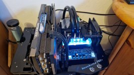
banchetto 101 ist super selten.Meins hatte ich damals gebraucht aus Frankreich bekommen.

Da musste ich erst mal die obere Platte polieren...aber man bekommt das gut hin.


RAM wieder unstable nachdem ich 3 Tage nicht am Rechner war. Musste die CPU VDDQ weiter hochdrehen damit es wieder stable läuft (2x 12k Karhu + TM5 Anta).
Frag mich ob das bei AMD auch so ein gefriemel ist... sonst wäre ein switch zu Zen5 ne Option.
 
DRAM WRITE to READ Delay L [15]
DRAM WRITE to READ Delay S [3]
Hi,
I completely missed over this message.
My bad

Soo this is bad
Writes in clock of 3 (write to pre), may or may not finish in time
It is inserted mid read (which is 8 clock, not 4) - soo middle is of course 4 clock not 2 or 3
The 2nd consecutive write:

Illustration
Code:
.... .... .... ....
RD.PR.... RD.AP....
.... WR.. .... ....
.... .... .... WR..
Read, 8 clock, read
Write can happen past first read, or 4 ticks before and after read
next write can not happen 4 ticks after read, but will happen with + 8 ticks delay (if there is no read in between)

If specific scenario is met
You get
+4pause, RD+8pause+Read+8pause
write + 4pause + 8 pause + write

Soo in technical terms
Read nop reads are 8 ticks, but only can happen if it jumps bankgroups
full roundtrip is 16 ticks (full burstlength)
Write , nop write
First write happens at 4 ticks, then its pause. If you write more data where no time needs to happen to (p)recharge rows or old targets
Then another write will happen after 8 more ticks are done. Then the actual write happens, because things need to align back to ticks of 8, after doing a write at half BurstChop8 aka 4 ticks
(soo together thats a distance of 12 ~ hence WRWR_SG can be 12 but shouldnt be)
_SG = same group = roundtrip.

This can happen because
8+8 + pause , 8+8
vs
4+ pause (we are at tick 8), more of 4 clock, (we are at tick 12) +4 , we are at tick 16 ~ back to 16, +16, +16 sync


Soo if above made any sense whatsoever
You need 4 ticks to pass // (all ticks pass at the same time, many commands happen at the same time)
soo read do their thing, and you can write to another away free space
WTR_S or so called _DG (different group, a short jump, no roundtrip waiting requirement)
^ will be WTRS = 4 , half clock of RRDS (8)

Now WTRL itself, is difficult to explain.
You know that after 4 ticks + catchup 4 ticks to be back on 8+8+8+8 rail
on the 2nd 8th tick, another read can happen.

Reads are heavy operations
It needs to backup data from row it accesses
Soo it only reads out what it really needs, while discharging the whole row where (other) data was.
It needs time to not only first fish away other important fish, then open drain valve,, collect what it needs, close drain valve, fill pool again with water till sensors say "waterlevel ok"
While pool fills start doing another work, wait for old to give "ok im usable again", put back fish, and move on.

Soo while first part is in processing state, another work begins in the timetable of 8 ticks, where it can operate.
It can not operate at 7th clock or 6th clock. UDIMM runs at 16 ticks roundtrip or 8 per whatever it has to do ~ burstchop 8 :)
Remember i said write back needs to happen
Writes are not destructive actions.
They can decide to happen at any time if there is space left for them and dont conflict with ongoing reads.

If data needs to be stored back to the same place, aka roundtrip (WTRL)
The moment it can do it, is when first pool is ok, soo 8++ clock
Then 2nd pool does finish its job (another 8 clock)
And if you have some more special vendor design ideas or overlapping ideas of lets say micron or samsung ~ another 8 clock

Soo WTRL at best is double RRDL, or sometimes 3* RRDL.
It can be any other value between 1.5* to 3* RRDL
But alignment is what matters.

Not because RAS to RAS (= RRD meaning) needs it. Reads from Writes are separated and an own thing
But because on the bigger picture, they will crossfight for processing priority and what happens is write just being delayed indefinitely.
Soo alignment is important :geek: but you may need to stop thinking about "book lecture of single operation".
// Likely why many tech space people confuse behavior.
// Too much focus on a single operation, without consideration of the trouble you cause by your action. Pre and past target timing.
DRAM RAS# to RAS# Delay L [8]
DRAM RAS# to RAS# Delay S [8]
See this
Soo correct behavior should be
DRAM WRITE to READ Delay L [16]
DRAM WRITE to READ Delay S [4]
With
tRDRD_sg_Runtime [16]
tRDRD_dg_Runtime [8]
tWRWR_sg [16]
tWRWR_dg [8]
RD 2 RD ~ roundtrip , 16 clock
RD 2 RD ~ fast jump, 8 clock

WR 2 WR ~ rountrip 12-16 clock, optimally 16. To have some breathing room
WR 2 WR ~ fast jump also 8 clock
Why not 4 ?
Because thats how memory operates. Go RDIMM + server boards for this, if you want two operations per single strobe (of 8).
// While one can be inserted at the middle, two can not. Two can happen between reads, but only if read is delayed,
// because 2nd write needs to be delayed to align back to 8+8+8+8 system.

Actions are done on strobe signal high. (most)
And strobe , runs in ticks of 8.
Can try what you want, but its 8. You can't call an apple a pear.
An apple grows to an apple,, even if you call it a pear. :geek:

UDIMM single row, can never do two things at the same time in one strobe.
Hence it can never be dual rank. Just dual sided with focus on access efficiency.
All DDR5 can jump bankgroups internally and subchannels semi-internally.
But per strobe its still one big operation with many round robin based orders.
 
Zuletzt bearbeitet:
Ring hits ICCMAX.

No way around undervolt to lower UncoreVID.
Or limiting max ring multiplier.
Hitting PL4 means throttle.
Sorry, ich bin eine Schneke :) so viele Zeit hatte ich keine. Arbeit, ich musste meinen Rechner umziehen, usw...
So, das war mein alte 13700k und total Default BIOS. Einfach eingegeben paar wichtige Werte für 8000 zum ausprobieren. Egal, ich wollte nur zeigen.

Weiter getestet, aber leider ohne kaltem Wasser. Wie normal.
So, es gibt zwei möglichkeit PL4 erreichen.
Eine ist, wenn Ring auto ist.
PL4 ist immer "Yes", und idle 48x, unter Last 45x.
Ich weiss es nicht wieso, normalleweisse Default BIOS muss gut sein.
Ok, im idle auch PL4 limit, wenn kein Amper fliest.

Andere Version ist, wenn ich Ring manuel begrenze.
Es gibt nicht mehr. Unter voll Last zB.: Y, kein PL4 limit.
Aber im idle, manchmal blinkt "Yes". Ich habe bis 47x getested, wenn Y oder egal was lauft, kein PL4 ist.

Bild PL4 Test

Nach dem Restart hab ich sofort Hwinfo gestartet, wir können noch die max Frequ idle auch sehen, danach 800MHz idle, und zwei mal war PL4 für kurze Zeit. Ohne Last.
Nacher habe ich Y gestartet, PL4 unter Y lauft kommt nie zurück.

Das ist für PL4 Thema.


Anders:

Ich habe noch etwas getan in meinem Freizeit.
Immernoch der klein Bruder, der 13700k ist drin.
Ram oc, ich bin sicher, dass 8000 Profil gut ist.
Beim 14900k, und jetzt 13700k Fehler ist gleiche.
Es bedeutet, Fehler komt von mir.
Jetzt ich kann es zeigen. Visual sehen wir besser.
Immer VT3. ...
Es ist nicht VT3 error, es ist zwischen Testen die kurze Zeit. Idle Spannung ist zu niedrig.
VST will starten, und immer da.

Bild1 ac53x, 2 Kerne 54x

Ok, das zwei Kerne Boost abgeschnitten, max 53x kann sein.

Bild2, ~0.65V idle ist nicht so viel, Crash wenn switch Test

Naja, habe ich mit Curve angefangen, wie beim 14900k.
Idle (800-2400MHz) fast 0.8V eingestellt. (~0.76V)
Ich wollte das nicht, daß es wegen zu niedrig idle Spannung nochmal stürtz ab.

Bonus Bild unter Last

Knapp 90 minute nicht geschafft.
Aber jetzt, es ist eine "gute Crash", weil genau in mitte dem VST.
Es bedeutet für mich, ich kann Speielen mit Spannungen, es ist ram oc Crash, nicht cpu Fehler.

80 min vst/vt3 8000c36 46 66

Ich bin schon zu frieden mit diesem Profil, mehr brauche ich nicht, stabilität werde ich noch später repairen.

Danke nochmal die viele gute Infos
 
Jetzt mal ernsthaft ich komme immer noch nicht hinter die kack Voltages kann mir die mal einer Vernünftig erklären ich finde wirklich nichts gescheites.

- IMC VDD ist doch die Spannung des CPU Memory Controller?
- VCCSA ist sowie North/ Southbridge Chip?
- Das IVR TX VDDQ ist was?
- VDD ist eine alleinige Spannung für RAM?
- VDDQ und VDDQ TX Spannung ist bei mir Synchron. Also wenn ich VDDQ im BIOS änder zieht sie die TX mit, i guees das ist diese echte XMP OC Spannung wie DDR4 Ram Voltage oder?
- VDD Sollte eigentlich immer 200-300 mV mehr haben als VDDQ?
 
I've been having issues getting 8400 stable on this chip through multiple kits and I'm no sure where to go next, everything I've tried yet has failed, at most I've gotten it stable for 26min in ycruncher but that was only for 1 restart and then I can't more than pass 1 loop.

I'm using TG Xtreem 2x24GB kit

this 8267 profile is stable with 1.12 SA, 1.3Tx, and 1.4MC so not sure why I'm having so much issues with 8400 and above.


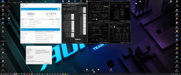
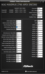
Wko3ZJxlUE.pngVXd7svNvx3.pngHj147CPGU8.pngdzbOzI2mgl.png
 
Hello @Veii

I was a bit tired of the unsuccessful attempts of stabilizing 8600, so made a 8533C36 profile.
I used the same Voltages as a base, only VDD bumped to 1.58V.
Passed TM5 for the first try, but Y was no good.

Képernyőkép 2024-01-23 070911.png


So I thought maybe raising MC to 1.537V would help a little. This give me one notch higher (+20mV) Voltage under load.
And here we have it!
1706001588710.png


Now I have this stable, I will try my 8600 profile with the same MC_VDD later.

Please don't check the bitrates I was working on the other screen during the test (I know, I am crazy, but I have some tight deadlines and couldn't resist to this profile)
 
Zuletzt bearbeitet:
Schon geil.

Kannst mal vst laufen lassen? Also mit dem 14er bekomme ich da nichts hin 🤣. Der einzige der das bei 8400 schafft ist mein 14600kf.
 
Gigabyte Z790 AORUS Tachyon
Sehr cool!
Schön zu sehen, dass es doch noch Leute gibt, die Gigabyte eine Chance geben. In den meisten Foren kann man nur nachlesen, wie alle das Gleiche mit dem gleichen Board von Asus machen und dafür alle einen Keks wollen.

Ich bin mal gespannt, wie weit das Aorus Tachyon kommt. Es dauert sicher noch ein paar Monate, bin die ersten 8600MT bzw. 9000MT/s für Desktop kommen.

Zu meinem Problem nochmal, ich weiß leider nicht, wo ich an welcher Schraube drehen muss, um 7600MT zum Laufen zu bekommen. Irgendwelche Vorschläge?

Das Bios von meinem Board dürfte sich nur sehr geringfügig vom Tachyon unterscheiden. In dem Online-Review habe keine Unterschiede sehen können. Soll heißen, die Einstellungen im Tachyon Bios sind auch da, wo meine sind.

Ich wollte mit meinem 13700K mein 7200MT Kit auf 7600MT übertakten, aber ich weiß nicht, ob das Board, die CPU oder die Speicher da limitieren. Einzel schaffen diese die 7600MT locker.

Irgendeine Idee?
 
Sehr gute Hilfe bei Gigabyte : https://yujihw.com/

Einfach auf Deutsch übersetzen .......Seite 1 und 4 gibt es gute RAM-Einstellungen auf für ein 4-DIMM Board

Ich habe vor dem Tachyon das Z790 Master gehabt und da habe ich auch 8000 na sagen wir mal 90% stabil bekommen.

Mit meiner jetzigen Erfahrung bestimmt 100 %
 
Schon geil.

Kannst mal vst laufen lassen?
+vt3

Audigy arbeitet grad an den H24M

 
Nicht mal einen loop vt3 🤣. Vst schaff ich schon einige aber vt3 null.
Mit dem einen Chip was ich da hatte konnte man was anfangen, ist aber schon verkauft :d CPU 55/43/45, CKE Auto, war nur ein Kurztest

cachedImage.png
 
Ycruncher normal ist echt kein thema mit dem Chip. Vst vt3 knallt aber übelst raus wenn man mal nur eben on the fly was macht.

Da kann ich auch an Timings und Spannungen drehen wie ich will. Shitty daily imc bleibt nen shitty daily imc 🤣. War schon richtig den guten imc auf dem 13er im daily zu halten.
 
Holy trinity :bigok:

Thanks @Veii for giving some guidance

What do you guys think, is there chance for 8400Mhz? Or should it fine tune this one and call it a day.

I have 80c temp limit as Im currently on 19€ heatsink temporarily, until I get my watercool gear together lol

Ps. Is there parameter for Y that it won't close the window after -TL is reached? It ran 2 hours already in the morning but didnt realize, that it will close the window after time limit is reached so I ran it again so I can share screenshot :d

Näyttökuva 2024-01-23 200217.png
 
Hardwareluxx setzt keine externen Werbe- und Tracking-Cookies ein. Auf unserer Webseite finden Sie nur noch Cookies nach berechtigtem Interesse (Art. 6 Abs. 1 Satz 1 lit. f DSGVO) oder eigene funktionelle Cookies. Durch die Nutzung unserer Webseite erklären Sie sich damit einverstanden, dass wir diese Cookies setzen. Mehr Informationen und Möglichkeiten zur Einstellung unserer Cookies finden Sie in unserer Datenschutzerklärung.


Zurück
Oben Unten refresh