[Sammelthread] AMD K7 - Sockel A (462)

nach dcen Aktionen vonBschicht86, was die"Reparatur von RAm angeht", mache ich mir weniger sorgen gewisse Chips auf gewisse Platinen zu bekommen :d
Ja, das wäre eine Möglichkeit. Ich habe mir 4x 1GB ECC Riegel mit diesen Chips geordert. Ein Riegel davon arbeitet zuverlässig auf einem K7S8X-E @ 200MHz / 2-2-2-9
 
Wenn Du diese Anzeige nicht sehen willst, registriere Dich und/oder logge Dich ein.
Interessant sind die Hynix doch eh nur als 512er. Ergo bleiben pro 1gb Stick 8 Chips nutzbar und 10 Chips Rest. Das wäre doch super um die zu binnen... Ich mein ja nur... :d Und das SPD auf non-ECC zu programmieren und zwei der 18 Chips zu entfernen ist jetzt nicht die große Sache.
 
Aus mir ääääh "unbekannten Gründen" sind nun Riegel bei Ram-Co ausverkauft... :fresse2: Parallel habe ich mir ein paar alte Sticks zum Üben aus dem Container gezogen :d
 
Aus mir ääääh "unbekannten Gründen" sind nun Riegel bei Ram-Co ausverkauft... :fresse2: Parallel habe ich mir ein paar alte Sticks zum Üben aus dem Container gezogen :d
Gute Sache! Ich bin dann mal auf Ergebnisse gespannt. :bigok:
 
So, the board boots again. But first without Tictac. I want to prepare that in peace and I still have to integrate the SIL rom.

Attached is the "FK" bios with the 4384 ROM for the SIL chip. This works with booting SATA III SSDs.

With the older versions, the SSD was recognized by the SIL chip, but booting was not possible.
Hi, I also have a Gigabyte 7n400 Pro2 rev.2.0 and the FK BIOS, thanks for posting the latest FK bios with integrated SiL 3512 latest bios - I will give that a go tomorrow before doing a fresh Windows XP install on my retro PC Build.
Did you ever integrate the TicTac mod into the FK Bios with the 4384 ROM for Sil chip ?

P.S. Sorry for typing in English, my German remembers school days and is too rusty :)

@digitalbath

 
Did you ever integrate the TicTac mod into the FK Bios with the 4384 ROM for Sil chip ?
I have no clue what Tictac did with his mod. I would expect, that he would like to change the romsips, but as far as I see the mod BIOS still uses default (Nvidia) romsips. Maybe I found the wrong version. Changing the Sil firmware is not difficult. I can do it for you. I can also do a romsip (with L12) mod if you want.

P.S. Sorry for typing in English, my German remembers school days and is too rusty :)
Not a problem for me. :)
 
I have no clue what Tictac did with his mod. I would expect that he would like to change the romsips, but as far as I see the mod BIOS still uses default (Nvidia) romsips. Maybe I found the wrong version. Changing the Sil firmware is not difficult. I can do it for you. I can also do a romsip (with L12) mod if you want.


Not a problem for me.:)
Thanks, the romsip is it the updated chipset/ram timing table for better overclocking? Yes Please :)

The attached zip is of the FK BIOS for this board with SIL 3512 v4.3.84 already integrated by Tsk

Thanks
 

Anhänge

  • BIOS-003512-xxx-4384.zip
    178,2 KB · Aufrufe: 63
Thanks, the romsip is it the updated chipset/ram timing table for better overclocking? Yes Please :)
Yes, romsips are chipset-ram-cpu timigns.

The attached zip is of the FK BIOS for this board with SIL 3512 v4.3.84 already integrated by Tsk
I used this SIL Firmware version for the following mods.
At first, I've modded the Tictac version and added the newer Sil version. As far as I see, this version is older then offical "tk" BIOS. You can find them as version "TM".
Then, I've modded the official (and newer) tk version. I've added the newer Sil Firmware version. Tictac also changed the LAN boot Firmware in his BIOS. I've integrated this version also in the tk mod.
For all mod BIOSes, I moved the FSB and DRAM settings to the voltage menu and I modified both BIOS versions with two often used romsips versions.

AS for all my modded BIOSes, using them at own risk!!!

 
Yes, romsips are chipset-ram-cpu timigns.


I used this SIL Firmware version for the following mods.
At first, I've modded the Tictac version and added the newer Sil version. As far as I see, this version is older then offical "tk" BIOS. You can find them as version "TM".
Then, I've modded the official (and newer) tk version. I've added the newer Sil Firmware version. Tictac also changed the LAN boot Firmware in his BIOS. I've integrated this version also in the tk mod.
For all mod BIOSes, I moved the FSB and DRAM settings to the voltage menu and I modified both BIOS versions with two often used romsips versions.

AS for all my modded BIOSes, using them at own risk!!!

Thank you very much! Can't wait to try it tomorrow, I'll report back how it went.
 
@digitalbath I report back that the custom bios works! thanks a lot man, the sata rom is updated, the options in the bios are re-organized and there's more of them when compared to standard ctrl + F1.
The only 2 things that are worth mentioning are:
- Windows XP would no longer start up from a sata drive and had to be freshly installed (not an issue as I was going to do it anyway)
- the AGP aperature size option disappeared
Thank you once again
 
I report back that the custom bios works! thanks a lot man, the sata rom is updated, the options in the bios are re-organized and there's more of them when compared to standard ctrl + F1.
The only 2 things that are worth mentioning are:
- Windows XP would no longer start up from a sata drive and had to be freshly installed (not an issue as I was going to do it anyway)
- the AGP aperature size option disappeared
Thank you once again
Many thanks for the reply! I hope I could help you.
I have no clue why the AGP aperature size disappeared. I will check this and post it here.
The Windows startup problem caused probably the APIC setting in the BIOS. If your OS is installed with the activated APIC option and you disable it, the OS will crash during the startup. Just a guess.
 
So I have one NF7 less for overclocking...
I wanted to tested a new CPU. I first did a 2400MHz 1.65v boot test and when posting the motherboard died.
CPU is working on my Epox.
Sad to hear this. Does the SB or NB gets hot? Maybe just a BIOS bug?

- the AGP aperature size option disappeared
I looked into the BIOS versions. The AGP aperature setting was still there but in a wrong place. I moved it to the correct menu. I replaced the mod BIOSes here:
 
I want to check if it is a bios chip failure. But that seems like a long shot. I have some reserve and pre programmed chips.
I can check how hot it was.

Oh and that 0346 IQYHA 2500+ XP-m , that was not that good. I had to use 1.75v to boot 2400MHz.
 
My guess is that this cpu is too old. iirc week 47/48 the production process was changed.

when posting the motherboard died.
Also got one NF7 which behaves the same. First it refused to boot, then it did and finally died while reporting the ram amount on POST. Never ran again after that. Still got it with me and might try again in the future. Currently it just reports ---- on the POST code card, so southbridge doesn't even start to execute the bios rom.

Same for my best A7N8X. That board doesn't execute the bios either... Also just ---- on POST code card.
 
My best nf7 is ling gone. That board was really good with fsb.

I see 0C on my post code card. But that is it.

I did not know the production process changed on that date.
 
I'm not 100% sure on the production week, but in the 4x weeks of 2003 AMD changed something, that's why the cpus made in 0351 to 0401 are good clockers.
If it begins to display codes, at least the southbridge is still alive. 0xC0 or 0x0C? 0x0C should be "initialize keyboard".
 
I'm not 100% sure on the production week, but in the 4x weeks of 2003 AMD changed something, that's why the cpus made in 0351 to 0401 are good clockers.

If it begins to display codes, at least the southbridge is still alive. 0xC0 or 0x0C? 0x0C should be "initialize keyboard".
I will check later. I switched to Epox for testing.
 
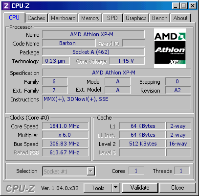
Got a second try on the stock NF7 v2.0. I'm waiting for some capacitors for a full recap and then will do voltmods. Mostly interested in highest stable FSB 1:1 with BH-5, but nevertheless tried to see how how I can go with 6:4 divider. Last time it stopped at 295, now - 306.83 and I saw 308 as well. Looks promising, probably my best nf2 board to date.

1706740709362.png


@auto660 so you want to replicate this adapter as I understand?
One thing to remind is that KT133 boards don't support A-XP so maybe this difference is what is preventing you from booting. Another thing is that Thunderbird CPUs were late and not all boards and BIOS versions might support them. So it's best to check TB support for Slot A and use TB socket A CPU. And even then they have different steppings AFAIR.
Just found this thread, looks very nice.

Anhang anzeigen 906817
It's been a while since i've been active here on the forums. Just didn't have the time and motivation to continue with the project, so it's been mostly stored away now in the hardware stash. But essentially i'm trying to replicate this adapter. But from the ground up using my own design, since this picture is the only documented thing left of all the Slot-A adapters that might have existed. As for the current state of this project...

The CPU gets initialized, the ROMSIP is transferred and (if i remember correctly) it's even confirmed by the CPU to the board that it was received/initialized successfully. All the clock signals and power-good signals seem to be there as well, with good signal quality/integrity. So that shouldn't be the problem, it's actually really nice that this part is good since signal integrity can be a b*tch to get right at these clockspeeds. I've also acquired a high-speed oscilloscope during this project which really helps with debugging stuff and checking if the signal waveforms look alright.

The main problem now is that the socket A CPU's won't start the data-communication bus in Open-Drain mode. Even the databus clock signals aren't activated, total silence on the bus traces. I've tried this with AMD751 based boards as well as with VIA KX133 based boards. With and without modded bioses. CPU-wise i've tried thunderbirds, durons, Thoroughbreds and Bartons. I've even put a Geode in there to check if the embedded stuff is a bit more willing to communicate via open-drain. But that was a no-go as well.

There is one motherboard though that uses the AMD751 Slot-A chipset while supporting Socket-A cpu's, with a modded bios it even works with the later Barton cores. I did some debugging work on that board and found out that it uses a customized ROMSIP to initialize the CPU in Push-Pull mode. In order to get the AMD751 chipset to initialize the CPU in Push-Pull mode, they've put the chipset permanently in debug-mode. This debug-mode allows the chipset to read a custom ROMSIP from an external EEPROM. So the board is using an external EEPROM to provide the correct ROMSIP to the CPU in order to make it work.

This motherboard (The Gigabyte GA-7IXE4, based on their Slot-A 7IXE variant) has an unpopulated jumper that makes the boards switch between the external and internal ROMSIP. I've added the jumper and switched between the ROMSIP's. The result was kinda expected, it will only boot with the external ROMSIP. The internal ROMSIP is a no-boot and gives the exact same behaviour as with the Slot-A adapter on a Slot-A board.

The high-speed oscilloscope came in very handy to see how the board and CPU behaves with both ROMSIP's. After scoping both the internal and external ROMSIP package we were able to decode them here on the forum. And this confirmed our assumptions. The external ROMSIP initialized the CPU in Push-Pull mode which works flawlessly. The internal ROMSIP on the other hand, initialized the CPU in Open-Drain mode which doesn't work. So here we have the reason why Gigabyte went through the trouble of putting the chipset in debug-mode and adding an external EEPROM. They probably had a whole stash of these chipsets left laying around when Socket-A was the hot new thing, so they went out of their way to still get a profit on them.

The next step would be to modify the ROMSIP such that the CPU is initialized in Push-Pull mode and see if the CPU tries to communicate. Unfortunately, both the AMD and VIA chipsets have a hardcoded ROMSIP that can't be changed. Putting the chipset in debug-mode and adding an EEPROM would require extensive mods to the motherboard and would be nearly impossible, especially without any further documentation about this debug-mode. It also defeats the use-case of this adapter and would only work on AMD based boards, not the VIA ones.

This brings us to the current state of the project. The only realistic solution to this would be to throw away the adapters and start a more viable project. uhh... i mean go on and find a way to initialize the CPU in push-pull mode without extensive mods to the motherboard. The only way to make this happen is to intercept the ROMSIP package and either modify or completely replace it. This will be a difficult task since it's a high speed signal (100MHz) and is timing sensitive in correlation with the incoming 100MHz PLL clock to the CPU.

So i've been looking for a solution. Back when Socket A launched, it would've been nearly impossible to make this happen in a price-competitive way, and with approval of AMD. Fortunately, we've advanced almost 25 years with technology and that approval of AMD is not really a thing anymore for the Slot/Socket A hardware. (I think/hope) It's also more of a gimmick, so price-competitiveness isn't too big of a thing now.

My first try was with the Raspberry Pi Pico (RP2040), unfortunately it seems like it's really struggling to make signals at a rate of 100MHz and it would be nearly impossible to time the signal correctly in correlation with the 100MHz PLL clocksignal. Fail.

My second try will be to use a FPGA that supports this kind of speeds and makes use of an external clock-input, so it can be driven by the 100MHz clock signal and keep near-perfect timing. Luckily these kind of FPGA's have become cheaply available throughout these 25 years so that would be an option worth to try. It even supports higher clockspeeds, and since it would be coupled to the CPU PLL clock, FSB/bus overclocking should stay possible from a theoretical standpoint. Actually, i've already ordered an FPGA board a while ago that's been sitting in the stash here for a while now.

Unfortunately i don't have time (yet) to try and make it work with the FPGA. But it's still something i want to do in the coming year. So the project isn't dead (yet), but it's gonna take some time to make the next big step.

I also want to thank everyone who helped here for their help to make this project happen. :-)
 
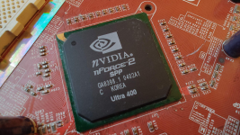
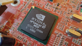
Small contribution to the list. This is the 306MHz stock board. Notice both NB and SB are Korean, not sure if that is relevant or just the production date.

NF7 v2.0, PCB version 0.52, plastic socket lever, blue DRAM slots
Northbridge: 0402 A1 SPP Ultra400 KOREA
Southbridge: 0346 A4 MCP KOREA
S/N: RA890414060094604
 

Anhänge

  • 1706882855072.png
    1706882855072.png
    1,6 MB · Aufrufe: 135
  • 1706882900571.png
    1706882900571.png
    1,8 MB · Aufrufe: 119
Although i technically don't really have time for this... I've started to invest some time into getting familiar with VHDL, the programming language for FPGA's. Also dug into the AMD datasheets again to freshen up some memory about the whole ROMSIP transfer procedure. The ROMSIP is transferred via the CONNECT data line, which is also used during power-down modes such as sleep mode. So that's fun.

Although this data line got multiple functions, it should still be possible to replace the ROMSIP package using a FPGA. The FPGA will have to act as a pass-through though once the ROMSIP has been sent, otherwise it will probably interfere with other system processes such as sleep modes which also use the CONNECT data line.

The downside of using a FPGA as a pass-through is that each signal is delayed by at least one clockcycle, the FPGA first has to receive and register the signal state before it is able to send it to the CPU. Luckily it seems like the CONNECT data line isn't that timing sensitive. As long as the bits are in sync with the system clock it should be alright, having one or two clockcycles of delay shouldn't make things unhappy. At least that's what i can make up from the limited amount of available documentation.

The next step would be to make the VHDL program and test it in a VHDL simulator. Once that's done i'll have to prepare all the hardware again and implement the FPGA somewhere between the CONNECT line. Hopefully the signal integrity won't be affected too much by routing it through the FPGA board using regular wires. :unsure:
 
One more thing... The KX133 seems to have a hardware strapping pin for the SysPushPull parameter. By using a pull-up (1) or pull-down (0) resistor the strapping can be adjusted. The pp/od parameter is strapped to the MAA4 pin of the SD-RAM interface so it's accessible through the ram slots, nice. :-)

The chipset also got predefined internal pull-up/down resistors for providing a default strapping. By default, the pp/od strap is pulled-down internally in the chipset, which corresponds to a 0. And weirdly enough, 0 corresponds to push-pull mode according to the chipset datasheet. So it should send a ROMSIP with the SysPushPull parameter enabled when the default strapping is used. (SysPushPull = 1)

And this is the point where stuff gets interesting. The Slot A boards use the default strapping for the pp/od parameter, as a result they should send a ROMSIP with the SysPushPull parameter enabled. But they still send a ROMSIP with the SysPushPull parameter disabled. I've checked the MAA4 pin with a multimeter and looked through some Slot-A board schematics, both confirmed that the default strapping is used on this pin. No external strapping resistor is used...

Out of curiousity, i started looking at some KT133 Socket-A board schematics. The KT133 chipset should be virtually the same as the KX133 chipset, just a revised variant which is optimized for Socket A. So register and pinout-wise, they should be the same. And surprisingly, these KT133 boards actually use an additional external pull-down resistor on the MAA4 strapping pin. This shouldn't be needed since the default chipset strapping already provides an internal pull-down resistor. Which makes me think that the datasheet is incorrect about the default pp/od strapping state.

So i'm going to add this external pull-down resistor to the MAA4 strapping pin on one of my KX133 Slot-A boards and probe the ROMSIP again. The datasheet tells me the external resistor isn't needed, yet the board vendors opted to add it anyway on their Socket-A KT133 boards. Which operate in Push-Pull mode. It would be great if this simple modification enables the SysPushPull parameter on KX133-based boards.

To be continued...
 
Hardwareluxx setzt keine externen Werbe- und Tracking-Cookies ein. Auf unserer Webseite finden Sie nur noch Cookies nach berechtigtem Interesse (Art. 6 Abs. 1 Satz 1 lit. f DSGVO) oder eigene funktionelle Cookies. Durch die Nutzung unserer Webseite erklären Sie sich damit einverstanden, dass wir diese Cookies setzen. Mehr Informationen und Möglichkeiten zur Einstellung unserer Cookies finden Sie in unserer Datenschutzerklärung.


Zurück
Oben Unten refresh