[Sammelthread] Intel DDR5 RAM OC Thread

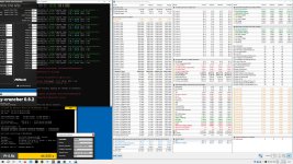
Neu BIOS fuer weisse Apex (2002) finde ich besser. Mein 8000C36-46-66 war nie in leben Y stable. Letzte Zeit konnte ich max 10 min laufen lassen. Immer VT3 Fehler.
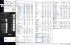
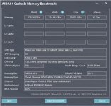
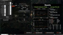
Update gemacht, sofort 30 minute lang ging. TM5 ist immer stable, egal was fuer eine Spannungen. Immer VT3...
Ich denke, es liegt an CPU quality. OC Profil gehts gut ohne Problem 24/7.
Lange Zeit habe ich schon aufgehoert mit RAM OC, nur wegen neuem BIOS getestet habe. Halbe Stunde ist so was :)
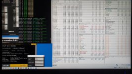
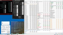
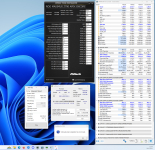
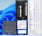
Mit dem Handy genau vor dem Fehler unter Last ein Bild gemacht. Knapp...
Naja, schwach CPU oder irgendwas. B Version, ich bin Noob :)
Man kann es nutzen in Alltags ohne Problem.
[2024/02/27 00:28:00]
Ai Overclock Tuner [Manual]
BCLK Frequency [100.0000]
PCIE Frequency [100.0000]
Intel(R) Adaptive Boost Technology [Auto]
ASUS MultiCore Enhancement [Enabled – Remove All limits (90°C)]
SVID Behavior [Trained]
BCLK Frequency : DRAM Frequency Ratio [100:100]
Memory Controller : DRAM Frequency Ratio [1:2]
DRAM Frequency [DDR5-8000MHz]
Performance Core Ratio [By Core Usage]
1-Core Ratio Limit [60]
2-Core Ratio Limit [59]
3-Core Ratio Limit [58]
4-Core Ratio Limit [57]
5-Core Ratio Limit [57]
6-Core Ratio Limit [56]
7-Core Ratio Limit [55]
8-Core Ratio Limit [55]
Performance Core0 Specific Ratio Limit [Auto]
Performance Core0 specific Voltage [Auto]
Performance Core1 Specific Ratio Limit [Auto]
Performance Core1 specific Voltage [Auto]
*Performance Core2 Specific Ratio Limit [Auto]
Performance Core2 specific Voltage [Auto]
*Performance Core3 Specific Ratio Limit [Auto]
Performance Core3 specific Voltage [Auto]
Performance Core4 Specific Ratio Limit [Auto]
Performance Core4 specific Voltage [Auto]
Performance Core5 Specific Ratio Limit [Auto]
Performance Core5 specific Voltage [Auto]
Performance Core6 Specific Ratio Limit [Auto]
Performance Core6 specific Voltage [Auto]
Performance Core7 Specific Ratio Limit [Auto]
Performance Core7 specific Voltage [Auto]
Efficient Core Ratio [By Core Usage]
Efficient Turbo Ratio Limit 1 [44]
Efficient Turbo Ratio Cores 1 [Auto]
Efficient Core Group0 Specific Ratio Limit [Auto]
Efficient Core Group0 specific Voltage [Auto]
Efficient Core Group1 Specific Ratio Limit [Auto]
Efficient Core Group1 specific Voltage [Auto]
Efficient Core Group2 Specific Ratio Limit [Auto]
Efficient Core Group2 specific Voltage [Auto]
Efficient Core Group3 Specific Ratio Limit [Auto]
Efficient Core Group3 specific Voltage [Auto]
AVX2 [Auto]
AVX2 Ratio Offset to per-core Ratio Limit [Auto]
AVX2 Voltage Guardband Scale Factor [Auto]
Maximus Tweak [Mode 2]
DRAM CAS# Latency [36]
DRAM RAS# to CAS# Delay Read [46]
DRAM RAS# to CAS# Delay Write [26]
DRAM RAS# PRE Time [46]
DRAM RAS# ACT Time [66]
DRAM Command Rate [2N]
DRAM RAS# to RAS# Delay L [12]
DRAM RAS# to RAS# Delay S [8]
DRAM REF Cycle Time 2 [544]
DRAM REF Cycle Time Same Bank [480]
DRAM Refresh Interval [131071]
DRAM WRITE Recovery Time [24]
DRAM READ to PRE Time [12]
DRAM FOUR ACT WIN Time [32]
DRAM WRITE to READ Delay L [24]
DRAM WRITE to READ Delay S [8]
DRAM CKE Minimum Pulse Width [20]
DRAM Write Latency [34]
Ctl0 dqvrefup [170]
Ctl0 dqvrefdn [88]
Ctl0 dqodtvrefup [Auto]
Ctl0 dqodtvrefdn [Auto]
Ctl1 cmdvrefup [Auto]
Ctl1 ctlvrefup [Auto]
Ctl1 clkvrefup [Auto]
Ctl1 ckecsvrefup [Auto]
Ctl2 cmdvrefdn [Auto]
Ctl2 ctlvrefdn [Auto]
Ctl2 clkvrefdn [Auto]
Read Equalization RxEq Start Sign [-]
Read Equalization RxEq Start [Auto]
Read Equalization RxEq Stop Sign [-]
Read Equalization RxEq Stop [Auto]
ODT_READ_DURATION [Auto]
ODT_READ_DELAY [Auto]
ODT_WRITE_DURATION [Auto]
ODT_WRITE_DELAY [Auto]
DQ RTT WR [40 DRAM Clock]
DQ RTT NOM RD [40 DRAM Clock]
DQ RTT NOM WR [34 DRAM Clock]
DQ RTT PARK [34 DRAM Clock]
DQ RTT PARK DQS [34 DRAM Clock]
GroupA CA ODT [240 DRAM Clock]
GroupA CS ODT [0 DRAM Clock]
GroupA CK ODT [0 DRAM Clock]
GroupB CA ODT [60 DRAM Clock]
GroupB CS ODT [40 DRAM Clock]
GroupB CK ODT [40 DRAM Clock]
Pull-up Output Driver Impedance [48 DRAM Clock]
Pull-Down Output Driver Impedance [40 DRAM Clock]
DQ RTT WR [40 DRAM Clock]
DQ RTT NOM RD [40 DRAM Clock]
DQ RTT NOM WR [34 DRAM Clock]
DQ RTT PARK [34 DRAM Clock]
DQ RTT PARK DQS [34 DRAM Clock]
GroupA CA ODT [240 DRAM Clock]
GroupA CS ODT [0 DRAM Clock]
GroupA CK ODT [0 DRAM Clock]
GroupB CA ODT [60 DRAM Clock]
GroupB CS ODT [40 DRAM Clock]
GroupB CK ODT [40 DRAM Clock]
Pull-up Output Driver Impedance [40 DRAM Clock]
Pull-Down Output Driver Impedance [48 DRAM Clock]
Round Trip Latency Init Value MC0 CHA [Auto]
Round Trip Latency Max Value MC0 CHA [Auto]
Round Trip Latency Offset Value Mode Sign MC0 CHA [-]
Round Trip Latency Offset Value MC0 CHA [Auto]
Round Trip Latency Init Value MC0 CHB [Auto]
Round Trip Latency Max Value MC0 CHB [Auto]
Round Trip Latency Offset Value Mode Sign MC0 CHB [-]
Round Trip Latency Offset Value MC0 CHB [Auto]
Round Trip Latency Init Value MC1 CHA [Auto]
Round Trip Latency Max Value MC1 CHA [Auto]
Round Trip Latency Offset Value Mode Sign MC1 CHA [-]
Round Trip Latency Offset Value MC1 CHA [Auto]
Round Trip Latency Init Value MC1 CHB [Auto]
Round Trip Latency Max Value MC1 CHB [Auto]
Round Trip Latency Offset Value Mode Sign MC1 CHB [-]
Round Trip Latency Offset Value MC1 CHB [Auto]
Round Trip Latency MC0 CHA R0 [Auto]
Round Trip Latency MC0 CHA R1 [Auto]
Round Trip Latency MC0 CHA R2 [0]
Round Trip Latency MC0 CHA R3 [0]
Round Trip Latency MC0 CHA R4 [0]
Round Trip Latency MC0 CHA R5 [0]
Round Trip Latency MC0 CHA R6 [0]
Round Trip Latency MC0 CHA R7 [0]
Round Trip Latency MC0 CHB R0 [Auto]
Round Trip Latency MC0 CHB R1 [Auto]
Round Trip Latency MC0 CHB R2 [0]
Round Trip Latency MC0 CHB R3 [0]
Round Trip Latency MC0 CHB R4 [0]
Round Trip Latency MC0 CHB R5 [0]
Round Trip Latency MC0 CHB R6 [0]
Round Trip Latency MC0 CHB R7 [0]
Round Trip Latency MC1 CHA R0 [Auto]
Round Trip Latency MC1 CHA R1 [Auto]
Round Trip Latency MC1 CHA R2 [0]
Round Trip Latency MC1 CHA R3 [0]
Round Trip Latency MC1 CHA R4 [0]
Round Trip Latency MC1 CHA R5 [0]
Round Trip Latency MC1 CHA R6 [0]
Round Trip Latency MC1 CHA R7 [0]
Round Trip Latency MC1 CHB R0 [Auto]
Round Trip Latency MC1 CHB R1 [Auto]
Round Trip Latency MC1 CHB R2 [0]
Round Trip Latency MC1 CHB R3 [0]
Round Trip Latency MC1 CHB R4 [0]
Round Trip Latency MC1 CHB R5 [0]
Round Trip Latency MC1 CHB R6 [0]
Round Trip Latency MC1 CHB R7 [0]
Early Command Training [Auto]
SenseAmp Offset Training [Auto]
Early ReadMPR Timing Centering 2D [Auto]
Read MPR Training [Auto]
Receive Enable Training [Auto]
Jedec Write Leveling [Auto]
Early Write Time Centering 2D [Auto]
Early Read Time Centering 2D [Auto]
Write Timing Centering 1D [Auto]
Write Voltage Centering 1D [Auto]
Read Timing Centering 1D [Auto]
Read Timing Centering with JR [Auto]
Dimm ODT Training* [Disabled]
Max RTT_WR [ODT Off]
DIMM RON Training* [Disabled]
Write Drive Strength/Equalization 2D* [Auto]
Write Slew Rate Training* [Auto]
Read ODT Training* [Disabled]
Comp Optimization Training [Auto]
Read Equalization Training* [Auto]
Read Amplifier Training* [Auto]
Write Timing Centering 2D [Auto]
Read Timing Centering 2D [Auto]
Command Voltage Centering [Auto]
Early Command Voltage Centering [Auto]
Write Voltage Centering 2D [Auto]
Read Voltage Centering 2D [Auto]
Late Command Training [Auto]
Round Trip Latency [Auto]
Turn Around Timing Training [Auto]
CMD CTL CLK Slew Rate [Auto]
CMD/CTL DS & E 2D [Auto]
Read Voltage Centering 1D [Auto]
TxDqTCO Comp Training* [Auto]
ClkTCO Comp Training* [Auto]
TxDqsTCO Comp Training* [Auto]
VccDLL Bypass Training [Auto]
CMD/CTL Drive Strength Up/Dn 2D [Auto]
DIMM CA ODT Training [Auto]
PanicVttDnLp Training* [Auto]
Read Vref Decap Training* [Auto]
Vddq Training [Disabled]
Duty Cycle Correction Training [Auto]
Periodic DCC [Auto]
Rank Margin Tool Per Bit [Auto]
DIMM DFE Training [Auto]
EARLY DIMM DFE Training [Auto]
Tx Dqs Dcc Training [Auto]
DRAM DCA Training [Auto]
Write Driver Strength Training [Auto]
Rank Margin Tool [Auto]
Memory Test [Auto]
DIMM SPD Alias Test [Auto]
Receive Enable Centering 1D [Auto]
Retrain Margin Check [Auto]
Write Drive Strength Up/Dn independently [Auto]
LPDDR DqDqs Re-Training [Auto]
Margin Check Limit [Disabled]
tRDRD_sg_Training [Auto]
tRDRD_sg_Runtime [16]
tRDRD_dg_Training [Auto]
tRDRD_dg_Runtime [8]
tRDWR_sg [20]
tRDWR_dg [20]
tWRWR_sg [16]
tWRWR_dg [8]
tWRRD_sg [Auto]
tWRRD_dg [Auto]
tRDRD_dr [0]
tRDRD_dd [0]
tRDWR_dr [0]
tRDWR_dd [0]
tWRWR_dr [0]
tWRWR_dd [0]
tWRRD_dr [0]
tWRRD_dd [0]
tRPRE [Auto]
tWPRE [Auto]
tWPOST [Auto]
tWRPRE [Auto]
tPRPDEN [Auto]
tRDPDEN [Auto]
tWRPDEN [Auto]
tCPDED [20]
tREFIX9 [Auto]
Ref Interval [Auto]
tXPDLL [Auto]
tXP [30]
tPPD [2]
tCCD_L_tDLLK [Auto]
tZQCAL [Auto]
tZQCS [Auto]
OREF_RI [Auto]
Refresh Watermarks [High]
Refresh Hp Wm [Auto]
Refresh Panic Wm [Auto]
Refresh Abr Release [Auto]
tXSDLL [Auto]
tZQOPER [Auto]
tMOD [Auto]
CounttREFIWhileRefEn [Auto]
HPRefOnMRS [Auto]
SRX Ref Debits [Auto]
RAISE BLK WAIT [Auto]
Ref Stagger En [Auto]
Ref Stagger Mode [Auto]
Disable Stolen Refresh [Auto]
En Ref Type Display [Auto]
Trefipulse Stagger Disable [Auto]
tRPab ext [Auto]
derating ext [Auto]
Allow 2cyc B2B LPDDR [Auto]
tCSH [Auto]
tCSL [Auto]
powerdown Enable [Auto]
idle length [Auto]
raise cke after exit latency [Auto]
powerdown latency [Auto]
powerdown length [Auto]
selfrefresh latency [Auto]
selfrefresh length [Auto]
ckevalid length [Auto]
ckevalid enable [Auto]
idle enable [Auto]
selfrefresh enable [Auto]
Address mirror [Auto]
no gear4 param divide [Auto]
x8 device [Auto]
no gear2 param divide [Auto]
ddr 1dpc split ranks on subch [Auto]
write0 enable [Auto]
MultiCycCmd [Auto]
WCKDiffLowInIdle [Auto]
PBR Disable [Auto]
PBR OOO Dis [Auto]
PBR Disable on hot [Auto]
PBR Exit on Idle Cnt [Auto]
tXSR [Auto]
Dec tCWL [Auto]
Add tCWL [Auto]
Add 1Qclk delay [Auto]
MRC Fast Boot [Disabled]
MCH Full Check [Auto]
Mem Over Clock Fail Count [3]
Training Profile [Auto]
RxDfe [Auto]
Mrc Training Loop Count [3]
DRAM CLK Period [Auto]
Dll_bwsel [Auto]
Controller 0, Channel 0 Control [Enabled]
Controller 0, Channel 1 Control [Enabled]
Controller 1, Channel 0 Control [Enabled]
Controller 1, Channel 1 Control [Enabled]
MC_Vref0 [Auto]
MC_Vref1 [Auto]
MC_Vref2 [Auto]
Fine Granularity Refresh mode [Auto]
SDRAM Density Per Die [Auto]
SDRAM Banks Per Bank Group [Auto]
SDRAM Bank Groups [Auto]
Dynamic Memory Boost [Disabled]
Realtime Memory Frequency [Disabled]
SA GV [Disabled]
Voltage Monitor [Die Sense]
VRM Initialization Check [Enabled]
CPU Input Voltage Load-line Calibration [Auto]
CPU Load-line Calibration [Level 4:Recommended for OC]
Synch ACDC Loadline with VRM Loadline [Disabled]
CPU Current Capability [140%]
CPU Current Reporting [Auto]
Core Voltage Suspension [Auto]
CPU VRM Switching Frequency [Auto]
VRM Spread Spectrum [Auto]
CPU Power Duty Control [Auto]
CPU Power Phase Control [Auto]
CPU Power Thermal Control [125]
CPU Core/Cache Boot Voltage [Auto]
CPU Input Boot Voltage [Auto]
PLL Termination Boot Voltage [Auto]
CPU Standby Boot Voltage [Auto]
Memory Controller Boot Voltage [Auto]
CPU Core Auto Voltage Cap [Auto]
CPU Input Auto Voltage Cap [Auto]
Memory Controller Auto Voltage Cap [Auto]
Fast Throttle Threshold [Auto]
Package Temperature Threshold [Auto]
Regulate Frequency by above Threshold [Auto]
IVR Transmitter VDDQ ICCMAX [Auto]
Unlimited ICCMAX [Auto]
CPU Core/Cache Current Limit Max. [400.00]
Long Duration Package Power Limit [320]
Package Power Time Window [Auto]
Short Duration Package Power Limit [330]
Dual Tau Boost [Disabled]
IA AC Load Line [0.32]
IA DC Load Line [Auto]
IA CEP [Disabled]
SA CEP [Disabled]
IA SoC Iccmax Reactive Protector [Disabled]
Inverse Temperature Dependency Throttle [Auto]
IA VR Voltage Limit [1580]
CPU SVID Support [Auto]
Cache Dynamic OC Switcher [Disabled]
TVB Voltage Optimizations [Disabled]
Enhanced TVB [Disabled]
Overclocking TVB [Disabled]
Overclocking TVB Global Temperature Offset Sign [+]
Overclocking TVB Global Temperature Offset Value [Auto]
Offset Mode Sign 1 [-]
V/F Point 1 Offset [0.01800]
Offset Mode Sign 2 [-]
V/F Point 2 Offset [0.00800]
Offset Mode Sign 3 [+]
V/F Point 3 Offset [0.03000]
Offset Mode Sign 4 [+]
V/F Point 4 Offset [0.04000]
Offset Mode Sign 5 [+]
V/F Point 5 Offset [0.03000]
Offset Mode Sign 6 [-]
V/F Point 6 Offset [0.03000]
Offset Mode Sign 7 [-]
V/F Point 7 Offset [0.10400]
Offset Mode Sign 8 [-]
V/F Point 8 Offset [0.10400]
Offset Mode Sign 9 [-]
V/F Point 9 Offset [0.15600]
Offset Mode Sign 10 [-]
V/F Point 10 Offset [0.15600]
Offset Mode Sign 11 [-]
V/F Point 11 Offset [0.15100]
Initial BCLK Frequency [Auto]
Runtime BCLK OC [Auto]
BCLK Amplitude [Auto]
BCLK Slew Rate [Auto]
BCLK Spread Spectrum [Auto]
Initial PCIE Frequency [Auto]
PCIE/DMI Amplitude [Auto]
PCIE/DMI Slew Rate [Auto]
PCIE/DMI Spread Spectrum [Auto]
Cold Boot PCIE Frequency [Auto]
Realtime Memory Timing [Disabled]
SPD Write Disable [TRUE]
PVD Ratio Threshold [Auto]
SA PLL Frequency Override [Auto]
BCLK TSC HW Fixup [Enabled]
Core Ratio Extension Mode [Disabled]
FLL OC mode [Auto]
UnderVolt Protection [Disabled]
Switch Microcode [Current Microcode]
Xtreme Tweaking [Disabled]
Core PLL Voltage [Auto]
GT PLL Voltage [Auto]
Ring PLL Voltage [Auto]
System Agent PLL Voltage [Auto]
Memory Controller PLL Voltage [Auto]
Efficient-core PLL Voltage [Auto]
CPU 1.8V Small Rail [Auto]
PLL Termination Voltage [Auto]
CPU Standby Voltage [Auto]
PCH 1.05V Voltage [Auto]
PCH 0.82V Voltage [Auto]
CPU Input Voltage Reset Voltage [Auto]
Eventual CPU Input Voltage [Auto]
Eventual Memory Controller Voltage [Auto]
Package Temperature Threshold [Auto]
Regulate Frequency by above Threshold [Auto]
Cooler Efficiency Customize [Keep Training]
Cooler Re-evaluation Algorithm [Normal]
Optimism Scale [100]
Ring Down Bin [Auto]
Min. CPU Cache Ratio [Auto]
Max. CPU Cache Ratio [49]
BCLK Aware Adaptive Voltage [Auto]
Actual VRM Core Voltage [Auto]
Global Core SVID Voltage [Auto]
Cache SVID Voltage [Auto]
CPU L2 Voltage [Auto]
CPU System Agent Voltage [Manual Mode]
- CPU System Agent Voltage Override [1.14000]
CPU Input Voltage [Auto]
High DRAM Voltage Mode [Enabled]
DRAM VDD Voltage [1.50000]
DRAM VDDQ Voltage [1.47000]
IVR Transmitter VDDQ Voltage [1.26500]
Memory Controller Voltage [1.36250]
MC Voltage Calculation Voltage Base [Auto]
VDD Calculation Voltage Base [Auto]
PMIC Voltages [Sync All PMICs]
SPD HUB VLDO (1.8V) [1.80000]
SPD HUB VDDIO (1.0V) [1.00000]
DRAM VDD Voltage [1.50000]
DRAM VDDQ Voltage [1.47000]
DRAM VPP Voltage [1.81500]
DRAM VDD Switching Frequency [1.50000]
DRAM VDDQ Switching Frequency [1.50000]
DRAM VPP Switching Frequency [1.50000]
DRAM Current Capability [7.87500]
PCI Express Native Power Management [Enabled]
Native ASPM [Disabled]
DMI Link ASPM Control [Disabled]
ASPM [Auto]
L1 Substates [Disabled]
DMI ASPM [Disabled]
DMI Gen3 ASPM [Disabled]
PEG - ASPM [Disabled]
PCI Express Clock Gating [Enabled]
Hardware Prefetcher [Enabled]
Adjacent Cache Line Prefetch [Enabled]
Intel (VMX) Virtualization Technology [Disabled]
Per P-Core Control [Disabled]
Per E-Core Control [Disabled]
Active Performance Cores [All]
Active Efficient Cores [All]
Hyper-Threading [Enabled]
Hyper-Threading of Core 0 [Enabled]
Hyper-Threading of Core 1 [Enabled]
Hyper-Threading of Core 2 [Enabled]
Hyper-Threading of Core 3 [Enabled]
Hyper-Threading of Core 4 [Enabled]
Hyper-Threading of Core 5 [Enabled]
Hyper-Threading of Core 6 [Enabled]
Hyper-Threading of Core 7 [Enabled]
Total Memory Encryption [Disabled]
Legacy Game Compatibility Mode [Disabled]
Boot performance mode [Auto]
Intel(R) SpeedStep(tm) [Enabled]
Intel(R) Speed Shift Technology [Enabled]
Intel(R) Turbo Boost Max Technology 3.0 [Enabled]
Turbo Mode [Enabled]
Acoustic Noise Mitigation [Disabled]
CPU C-states [Auto]
Thermal Monitor [Enabled]
Dual Tau Boost [Disabled]
VT-d [Disabled]
Memory Remap [Enabled]
Enable VMD controller [Enabled]
Map PCIE Storage under VMD [Disabled]
Map SATA Controller under VMD [Disabled]
M.2_1 Link Speed [Auto]
PCIEX16(G5)_1 Link Speed [Auto]
PCIEX16(G5)_2 Link Speed [Auto]
PCIEX1(G4) Link Speed [Auto]
PCIEX4(G4) Link Speed [Auto]
M.2_2 Link Speed [Auto]
DIMM.2_1 Link Speed [Auto]
DIMM.2_2 Link Speed [Auto]
SATA Controller(s) [Enabled]
Aggressive LPM Support [Disabled]
SMART Self Test [Enabled]
M.2_3 [Enabled]
M.2_3 Hot Plug [Disabled]
SATA6G_1 [Enabled]
SATA6G_1 Hot Plug [Disabled]
SATA6G_2 [Enabled]
SATA6G_2 Hot Plug [Disabled]
SATA6G_3 [Enabled]
SATA6G_3 Hot Plug [Disabled]
SATA6G_4 [Enabled]
SATA6G_4 Hot Plug [Disabled]
PTT [Enable]
Intel(R) Dynamic Tuning Technology [Disabled]
PCIE Tunneling over USB4 [Enabled]
Discrete Thunderbolt(TM) Support [Disabled]
Security Device Support [Enable]
SHA256 PCR Bank [Enabled]
Pending operation [None]
Platform Hierarchy [Enabled]
Storage Hierarchy [Enabled]
Endorsement Hierarchy [Enabled]
Physical Presence Spec Version [1.3]
Disable Block Sid [Disabled]
USB Host Controller Support [Disabled]
Password protection of Runtime Variables [Enable]
Above 4G Decoding [Enabled]
Resize BAR Support [Enabled]
SR-IOV Support [Disabled]
Legacy USB Support [Enabled]
XHCI Hand-off [Enabled]
SanDisk [Auto]
LAN_U32G2_1 [Enabled]
U32G1_E5 [Enabled]
U32G1_E6 [Enabled]
U32G1_E7 [Enabled]
U32G1_E8 [Enabled]
U32G2X2_C3 [Enabled]
U32G2_5 [Enabled]
U32G2_6 [Enabled]
U32G2_7 [Enabled]
U32G2_P8 [Enabled]
U32G2X2_C9 [Enabled]
U32G1_E1 [Enabled]
U32G1_E2 [Enabled]
U32G1_E3 [Enabled]
U32G1_E4 [Enabled]
Network Stack [Disabled]
Device [N/A]
Restore AC Power Loss [Power Off]
Max Power Saving [Disabled]
ErP Ready [Disabled]
Power On By PCI-E [Disabled]
Power On By RTC [Disabled]
USB Audio [Enabled]
Intel LAN [Enabled]
USB power delivery in Soft Off state (S5) [Disabled]
Connectivity mode (Wi-Fi & Bluetooth) [Enabled]
When system is in working state [All On]
Q-Code LED Function [Auto]
When system is in sleep, hibernate or soft off states [All On]
M.2_2 Configuration [Auto]
ASMedia USB 3.2 Controller_U32G1_E12 [Enabled]
ASMedia USB 3.2 Controller_U32G1_E34 [Enabled]
GNA Device [Disabled]
ASMedia Storage Controller [Enabled]
Windows Hot-plug Notification [Disabled]
ASPM Support [Disabled]
CPU Temperature [Monitor]
CPU Package Temperature [Monitor]
MotherBoard Temperature [Monitor]
VRM Temperature [Monitor]
Chipset Temperature [Monitor]
T_Sensor Temperature [Monitor]
DIMM.2 Sensor 1 Temperature [Monitor]
DIMM.2 Sensor 2 Temperature [Monitor]
Water In T Sensor Temperature [Monitor]
Water Out T Sensor Temperature [Monitor]
DIMM A1 Temperature [Monitor]
DIMM B1 Temperature [Monitor]
CPU Fan Speed [Monitor]
CPU Optional Fan Speed [Monitor]
Chassis Fan 1 Speed [Monitor]
Chassis Fan 2 Speed [Monitor]
Chassis Fan 3 Speed [Monitor]
Water Pump+ Speed [Monitor]
AIO Pump Speed [Monitor]
Flow Rate [Monitor]
CPU Core Voltage [Monitor]
12V Voltage [Monitor]
5V Voltage [Monitor]
3.3V Voltage [Monitor]
Memory Controller Voltage [Monitor]
CPU Fan Q-Fan Control [DC Mode]
CPU Fan Profile [Standard]
CPU Fan Q-Fan Source [CPU]
CPU Fan Step Up [Level 0]
CPU Fan Step Down [Level 4]
CPU Fan Speed Low Limit [200 RPM]
Chassis Fan 1 Q-Fan Control [Auto Detect]
Chassis Fan 1 Profile [Standard]
Chassis Fan 1 Q-Fan Source [CPU]
Chassis Fan 1 Step Up [Level 0]
Chassis Fan 1 Step Down [Level 0]
Chassis Fan 1 Speed Low Limit [200 RPM]
Chassis Fan 2 Q-Fan Control [PWM Mode]
Chassis Fan 2 Profile [Standard]
Chassis Fan 2 Q-Fan Source [Chipset]
Chassis Fan 2 Step Up [Level 0]
Chassis Fan 2 Step Down [Level 4]
Chassis Fan 2 Speed Low Limit [200 RPM]
Chassis Fan 3 Q-Fan Control [DC Mode]
Chassis Fan 3 Profile [Silent]
Chassis Fan 3 Q-Fan Source [CPU]
Chassis Fan 3 Step Up [Level 0]
Chassis Fan 3 Step Down [Level 0]
Chassis Fan 3 Speed Low Limit [200 RPM]
Water Pump+ Q-Fan Control [PWM Mode]
Water Pump+ Profile [Manual]
Water Pump+ Q-Fan Source [CPU]
Water Pump+ Step Up [Level 0]
Water Pump+ Step Down [Level 4]
Water Pump+ Speed Low Limit [Ignore]
Water Pump+ Point4 Temperature [70]
Water Pump+ Point4 Duty Cycle (%) [100]
Water Pump+ Point3 Temperature [50]
Water Pump+ Point3 Duty Cycle (%) [85]
Water Pump+ Point2 Temperature [40]
Water Pump+ Point2 Duty Cycle (%) [80]
Water Pump+ Point1 Temperature [25]
Water Pump+ Point1 Duty Cycle (%) [60]
AIO Pump Q-Fan Control [Auto Detect]
AIO Pump Profile [Full Speed]
CPU Temperature LED Switch [Enabled]
Launch CSM [Disabled]
OS Type [Other OS]
Secure Boot Mode [Custom]
Fast Boot [Enabled]
Next Boot after AC Power Loss [Fast Boot]
Boot Logo Display [Auto]
POST Delay Time [3 sec]
Bootup NumLock State [On]
Wait For 'F1' If Error [Enabled]
Option ROM Messages [Force BIOS]
Interrupt 19 Capture [Disabled]
AMI Native NVMe Driver Support [Enabled]
Setup Mode [Advanced Mode]
Boot Sector (MBR/GPT) Recovery Policy [Local User Control]
Next Boot Recovery Action [Skip]
BIOS Image Rollback Support [Enabled]
Publish HII Resources [Disabled]
Flexkey [Safe Boot]
Setup Animator [Disabled]
Load from Profile [1]
Profile Name [8000]
Save to Profile [1]
DIMM Slot Number [DIMM_A1]
Download & Install ARMOURY CRATE app [Disabled]
Download & Install MyASUS service & app [Disabled]
 

Anhänge

  • 20240227_012051.jpg
    20240227_012051.jpg
    1,5 MB · Aufrufe: 64
  • 8000-C36.jpg
    8000-C36.jpg
    759,7 KB · Aufrufe: 56
Zuletzt bearbeitet:
Wenn Du diese Anzeige nicht sehen willst, registriere Dich und/oder logge Dich ein.
I think the new BIOS for the white Apex (2002) is better. My 8000C36-46-66 was never stable in its life. Recently I was able to run it for a maximum of 10 minutes. Always VT3 error.
Updated, it worked immediately for 30 minutes. TM5 is always stable, no matter what the voltage. Always VT3...
I think it's due to CPU quality. OC profile works well without any problems 24/7.
I stopped using RAM OC for a long time, just because I was testing new BIOS. Half an hour is something like that:)
I took a picture with my cell phone under load right before the error occurred. Meager...
Well, weak CPU or something. B version, I'm a noob:)
You can use it in everyday life without any problems.
[2024/02/27 00:28:00]
Ai Overclock Tuner [Manual]
BCLK Frequency [100,0000]
PCIE Frequency [100,0000]
Intel(R) Adaptive Boost Technology [Auto]
ASUS MultiCore Enhancement [Enabled – Remove All limits (90°C)]
SVID Behavior [Trained]
BCLK Frequency : DRAM Frequency Ratio [100:100]
Memory Controller: DRAM Frequency Ratio [1:2]
DRAM Frequency [DDR5-8000MHz]
Performance Core Ratio [By Core Usage]
1-Core Ratio Limit [60]
2-Core Ratio Limit [59]
3-Core Ratio Limit [58]
4-Core Ratio Limit [57]
5-Core Ratio Limit [57]
6-Core Ratio Limit [56]
7-Core Ratio Limit [55]
8-Core Ratio Limit [55]
Performance Core0 Specific Ratio Limit [Auto]
Performance Core0 specific Voltage [Auto]
Performance Core1 Specific Ratio Limit [Auto]
Performance Core1 specific Voltage [Auto]
*Performance Core2 Specific Ratio Limit [Auto]
Performance Core2 specific Voltage [Auto]
*Performance Core3 Specific Ratio Limit [Auto]
Performance Core3 specific Voltage [Auto]
Performance Core4 Specific Ratio Limit [Auto]
Performance Core4 specific Voltage [Auto]
Performance Core5 Specific Ratio Limit [Auto]
Performance Core5 specific Voltage [Auto]
Performance Core6 Specific Ratio Limit [Auto]
Performance Core6 specific Voltage [Auto]
Performance Core7 Specific Ratio Limit [Auto]
Performance Core7 specific Voltage [Auto]
Efficient Core Ratio [By Core Usage]
Efficient Turbo Ratio Limit 1 [44]
Efficient Turbo Ratio Cores 1 [Auto]
Efficient Core Group0 Specific Ratio Limit [Auto]
Efficient Core Group0 specific Voltage [Auto]
Efficient Core Group1 Specific Ratio Limit [Auto]
Efficient Core Group1 specific Voltage [Auto]
Efficient Core Group2 Specific Ratio Limit [Auto]
Efficient Core Group2 specific Voltage [Auto]
Efficient Core Group3 Specific Ratio Limit [Auto]
Efficient Core Group3 specific Voltage [Auto]
AVX2 [Auto]
AVX2 Ratio Offset to per-core Ratio Limit [Auto]
AVX2 Voltage Guardband Scale Factor [Auto]
Maximus Tweak [Mode 2]
DRAM CAS# Latency [36]
DRAM RAS# to CAS# Delay Read [46]
DRAM RAS# to CAS# Delay Write [26]
DRAM RAS# PRE Time [46]
DRAM RAS# ACT Time [66]
DRAM Command Rate [2N]
DRAM RAS# to RAS# Delay L [12]
DRAM RAS# to RAS# Delay S [8]
DRAM REF Cycle Time 2 [544]
DRAM REF Cycle Time Same Bank [480]
DRAM Refresh Interval [131071]
DRAM WRITE Recovery Time [24]
DRAM READ to PRE Time [12]
DRAM FOUR ACT WIN Time [32]
DRAM WRITE to READ Delay L [24]
DRAM WRITE to READ Delay S [8]
DRAM CKE Minimum Pulse Width [20]
DRAM write latency [34]
Ctl0 dqvrefup[170]
Ctl0 dqvrefdn [88]
Ctl0 dqodtvrefup [Auto]
Ctl0 dqodtvrefdn [Auto]
Ctl1 cmdvrefup [Auto]
Ctl1 ctlvrefup [Auto]
Ctl1 clkvrefup [Auto]
Ctl1 ckecsvrefup [Auto]
Ctl2 cmdvrefdn [Auto]
Ctl2 ctlvrefdn [Auto]
Ctl2 clkvrefdn [Auto]
Read Equalization RxEq Start Sign [-]
Read Equalization RxEq Start [Auto]
Read Equalization RxEq Stop Sign [-]
Read Equalization RxEq Stop [Auto]
ODT_READ_DURATION [Auto]
ODT_READ_DELAY [Auto]
ODT_WRITE_DURATION [Auto]
ODT_WRITE_DELAY [Auto]
DQ RTT WR [40 DRAM Clock]
DQ RTT NOM RD [40 DRAM Clock]
DQ RTT NOM WR [34 DRAM Clock]
DQ RTT PARK [34 DRAM Clock]
DQ RTT PARK DQS [34 DRAM Clock]
GroupA CA ODT [240 DRAM Clock]
GroupA CS ODT [0 DRAM Clock]
GroupA CK ODT [0 DRAM Clock]
GroupB CA ODT [60 DRAM Clock]
GroupB CS ODT [40 DRAM Clock]
GroupB CK ODT [40 DRAM Clock]
Pull-up Output Driver Impedance [48 DRAM Clock]
Pull-Down Output Driver Impedance [40 DRAM Clock]
DQ RTT WR [40 DRAM Clock]
DQ RTT NOM RD [40 DRAM Clock]
DQ RTT NOM WR [34 DRAM Clock]
DQ RTT PARK [34 DRAM Clock]
DQ RTT PARK DQS [34 DRAM Clock]
GroupA CA ODT [240 DRAM Clock]
GroupA CS ODT [0 DRAM Clock]
GroupA CK ODT [0 DRAM Clock]
GroupB CA ODT [60 DRAM Clock]
GroupB CS ODT [40 DRAM Clock]
GroupB CK ODT [40 DRAM Clock]
Pull-up Output Driver Impedance [40 DRAM Clock]
Pull-Down Output Driver Impedance [48 DRAM Clock]
Round Trip Latency Init Value MC0 CHA [Auto]
Round Trip Latency Max Value MC0 CHA [Auto]
Round Trip Latency Offset Value Mode Sign MC0 CHA [-]
Round Trip Latency Offset Value MC0 CHA [Auto]
Round Trip Latency Init Value MC0 CHB [Auto]
Round Trip Latency Max Value MC0 CHB [Auto]
Round Trip Latency Offset Value Mode Sign MC0 CHB [-]
Round Trip Latency Offset Value MC0 CHB [Auto]
Round Trip Latency Init Value MC1 CHA [Auto]
Round Trip Latency Max Value MC1 CHA [Auto]
Round Trip Latency Offset Value Mode Sign MC1 CHA [-]
Round Trip Latency Offset Value MC1 CHA [Auto]
Round Trip Latency Init Value MC1 CHB [Auto]
Round Trip Latency Max Value MC1 CHB [Auto]
Round Trip Latency Offset Value Mode Sign MC1 CHB [-]
Round Trip Latency Offset Value MC1 CHB [Auto]
Round Trip Latency MC0 CHA R0 [Auto]
Round Trip Latency MC0 CHA R1 [Auto]
Round Trip Latency MC0 CHA R2 [0]
Round Trip Latency MC0 CHA R3 [0]
Round Trip Latency MC0 CHA R4 [0]
Round Trip Latency MC0 CHA R5 [0]
Round Trip Latency MC0 CHA R6 [0]
Round Trip Latency MC0 CHA R7 [0]
Round Trip Latency MC0 CHB R0 [Auto]
Round Trip Latency MC0 CHB R1 [Auto]
Round Trip Latency MC0 CHB R2 [0]
Round Trip Latency MC0 CHB R3 [0]
Round Trip Latency MC0 CHB R4 [0]
Round Trip Latency MC0 CHB R5 [0]
Round Trip Latency MC0 CHB R6 [0]
Round Trip Latency MC0 CHB R7 [0]
Round Trip Latency MC1 CHA R0 [Auto]
Round Trip Latency MC1 CHA R1 [Auto]
Round Trip Latency MC1 CHA R2 [0]
Round Trip Latency MC1 CHA R3 [0]
Round Trip Latency MC1 CHA R4 [0]
Round Trip Latency MC1 CHA R5 [0]
Round Trip Latency MC1 CHA R6 [0]
Round Trip Latency MC1 CHA R7 [0]
Round Trip Latency MC1 CHB R0 [Auto]
Round Trip Latency MC1 CHB R1 [Auto]
Round Trip Latency MC1 CHB R2 [0]
Round Trip Latency MC1 CHB R3 [0]
Round Trip Latency MC1 CHB R4 [0]
Round Trip Latency MC1 CHB R5 [0]
Round Trip Latency MC1 CHB R6 [0]
Round Trip Latency MC1 CHB R7 [0]
Early Command Training [Auto]
SenseAmp Offset Training [Auto]
Early ReadMPR Timing Centering 2D [Auto]
Read MPR Training [Auto]
Receive Enable Training [Auto]
Allc Write Leveling [Auto]
Early Write Time Centering 2D [Auto]
Early Read Time Centering 2D [Auto]
Write Timing Centering 1D [Auto]
Write Voltage Centering 1D [Auto]
Read Timing Centering 1D [Auto]
Read Timing Centering with JR [Auto]
Dimm ODT Training* [Disabled]
Max RTT_WR [ODT Off]
DIMM RON Training* [Disabled]
Write Drive Strength/Equalization 2D* [Auto]
Write Slew Rate Training* [Auto]
Read ODT Training* [Disabled]
Comp Optimization Training [Auto]
Read Equalization Training* [Auto]
Read Amplifier Training* [Auto]
Write Timing Centering 2D [Auto]
Read Timing Centering 2D [Auto]
Command Voltage Centering [Auto]
Early Command Voltage Centering [Auto]
Write Voltage Centering 2D [Auto]
Read Voltage Centering 2D [Auto]
Late Command Training [Auto]
Round Trip Latency [Auto]
Turn Around Timing Training [Auto]
CMD CTL CLK Slew Rate [Auto]
CMD/CTL DS & E 2D [Auto]
Read Voltage Centering 1D [Auto]
TxDqTCO Comp Training* [Auto]
ClkTCO Comp Training* [Auto]
TxDqsTCO Comp Training* [Auto]
VccDLL Bypass Training [Auto]
CMD/CTL Drive Strength Up/Dn 2D [Auto]
DIMM CA ODT Training [Auto]
PanicVttDnLp Training* [Auto]
Read Vref Decap Training* [Auto]
Vddq Training [Disabled]
Duty Cycle Correction Training [Auto]
Periodic DCC [Auto]
Rank Margin Tool Per Bit [Auto]
DIMM DFE Training [Auto]
EARLY DIMM DFE Training [Auto]
Tx Dqs Dcc Training [Auto]
DRAM DCA Training [Auto]
Write Driver Strength Training [Auto]
Rank Margin Tool [Auto]
Memory Test [Auto]
DIMM SPD Alias Test [Auto]
Receive Enable Centering 1D [Auto]
Retrain Margin Check [Auto]
Write Drive Strength Up/Dn independently [Auto]
LPDDR DqDqs Re-Training [Auto]
Margin Check Limit [Disabled]
tRDRD_sg_Training [Auto]
tRDRD_sg_Runtime [16]
tRDRD_dg_Training [Auto]
tRDRD_dg_Runtime [8]
tRDWR_sg[20]
tRDWR_dg [20]
tWRWR_sg [16]
tWRWR_dg [8]
tWRRD_sg [Auto]
tWRRD_dg [Auto]
tRDRD_dr [0]
tRDRD_dd [0]
tRDWR_dr [0]
tRDWR_dd [0]
tWRWR_dr [0]
tWRWR_dd [0]
tWRRD_dr [0]
tWRRD_dd [0]
tRPRE [Auto]
tWPRE [Auto]
tWPOST [Auto]
tWRPRE [Auto]
tPRPDEN [Auto]
tRDPDEN [Auto]
tWRPDEN [Auto]
tCPDED [20]
tREFIX9 [Auto]
Ref Interval [Auto]
tXPDLL [Auto]
tXP[30]
tPPD [2]
tCCD_L_tDLLK [Auto]
tZQCAL [Auto]
tZQCS [Auto]
OREF_RI [Auto]
Refresh Watermarks [High]
Refresh Hp Wm [Auto]
Refresh Panic Wm [Auto]
Refresh Abr Release [Auto]
tXSDLL [Auto]
tZQOPER [Auto]
tMOD [Auto]
CounttREFIWhileRefEn [Auto]
HPRefOnMRS [Auto]
SRX Ref Debits [Auto]
RAISE BLK WAIT [Auto]
Ref Stagger En [Auto]
Ref Stagger Mode [Auto]
Disable Stolen Refresh [Auto]
En Ref Type Display [Auto]
Trefipulse Stagger Disable [Auto]
tRPab ext [Auto]
derating ext [Auto]
Allow 2cyc B2B LPDDR [Auto]
tCSH [Auto]
tCSL [Auto]
powerdown Enable [Auto]
idle length [Auto]
raise cke after exit latency [Auto]
powerdown latency [Auto]
power down length [Auto]
selfrefresh latency [Auto]
selfrefresh length [Auto]
ckevalid length [Auto]
ckevalid enable [Auto]
idle enable [Auto]
selfrefresh enable [Auto]
Address mirror [Auto]
no gear4 param divide [Auto]
x8 device [Auto]
no gear2 param divide [Auto]
ddr 1dpc split ranks on subch [Auto]
write0 enable [Auto]
MultiCycCmd [Auto]
WCKDiffLowInIdle [Auto]
PBR Disable [Auto]
PBR OOO Dis [Auto]
PBR Disable on hot [Auto]
PBR Exit on Idle Cnt [Auto]
tXSR [Auto]
Dec tCWL [Auto]
Add tCWL [Auto]
Add 1Qclk delay [Auto]
MRC Fast Boot [Disabled]
MCH Full Check [Auto]
Mem Over Clock Fail Count [3]
Training Profiles [Auto]
RxDfe [Auto]
Mrc Training Loop Count [3]
DRAM CLK Period [Auto]
Dll_bwsel [Auto]
Controller 0, Channel 0 Control [Enabled]
Controller 0, Channel 1 Control [Enabled]
Controller 1, Channel 0 Control [Enabled]
Controller 1, Channel 1 Control [Enabled]
MC_Vref0 [Auto]
MC_Vref1 [Auto]
MC_Vref2 [Auto]
Fine Granularity Refresh mode [Auto]
SDRAM Density Per Die [Auto]
SDRAM Banks Per Bank Group [Auto]
SDRAM Bank Groups [Auto]
Dynamic Memory Boost [Disabled]
Realtime Memory Frequency [Disabled]
SA GV [Disabled]
Voltage Monitor [The Scythe]
VRM Initialization Check [Enabled]
CPU Input Voltage Load-line Calibration [Auto]
CPU Load-line Calibration [Level 4:Recommended for OC]
Synch ACDC Loadline with VRM Loadline [Disabled]
CPU Current Capability [140%]
CPU Current Reporting [Auto]
Core Voltage Suspension [Auto]
CPU VRM Switching Frequency [Auto]
VRM Spread Spectrum [Auto]
CPU Power Duty Control [Auto]
CPU Power Phase Control [Auto]
CPU Power Thermal Control [125]
CPU Core/Cache Boot Voltage [Auto]
CPU Input Boot Voltage [Auto]
PLL Termination Boot Voltage [Auto]
CPU Standby Boot Voltage [Auto]
Memory Controller Boot Voltage [Auto]
CPU Core Auto Voltage Cap [Auto]
CPU Input Auto Voltage Cap [Auto]
Memory Controller Auto Voltage Cap [Auto]
Fast Throttle Threshold [Auto]
Package Temperature Threshold [Auto]
Regulate Frequency by above Threshold [Auto]
IVR Transmitter VDDQ ICCMAX [Auto]
Unlimited ICCMAX [Auto]
CPU Core/Cache Current Limit Max. [400.00]
Long Duration Package Power Limit [320]
Package Power Time Window [Auto]
Short Duration Package Power Limit [330]
Dual Tau Boost [Disabled]
IA AC Load Line [0.32]
IA DC Load Line [Auto]
IA CEP [Disabled]
SA CEP [Disabled]
IA SoC Iccmax Reactive Protector [Disabled]
Inverse Temperature Dependency Throttle [Auto]
IA VR Voltage Limit [1580]
CPU SVID Support [Auto]
Cache Dynamic OC Switcher [Disabled]
TVB Voltage Optimizations [Disabled]
Enhanced TVB [Disabled]
Overclocking TVB [Disabled]
Overclocking TVB Global Temperature Offset Sign [+]
Overclocking TVB Global Temperature Offset Value [Auto]
Offset Mode Sign 1 [-]
V/F Point 1 Offset [0.01800]
Offset Mode Sign 2 [-]
V/F Point 2 Offset [0.00800]
Offset Mode Sign 3 [+]
V/F Point 3 Offset [0.03000]
Offset Mode Sign 4 [+]
V/F Point 4 Offset [0.04000]
Offset Mode Sign 5 [+]
V/F Point 5 Offset [0.03000]
Offset Mode Sign 6 [-]
V/F Point 6 Offset [0.03000]
Offset Mode Sign 7 [-]
V/F Point 7 Offset [0.10400]
Offset Mode Sign 8 [-]
V/F Point 8 Offset [0.10400]
Offset Mode Sign 9 [-]
V/F Point 9 Offset [0.15600]
Offset Mode Sign 10 [-]
V/F Point 10 Offset [0.15600]
Offset Mode Sign 11 [-]
V/F Point 11 Offset [0.15100]
Initial BCLK Frequency [Auto]
Runtime BCLK OC [Auto]
BCLK Amplitude [Auto]
BCLK Slew Rate [Auto]
BCLK Spread Spectrum [Auto]
Initial PCIE Frequency [Auto]
PCIE/DMI Amplitude [Auto]
PCIE/DMI Slew Rate [Auto]
PCIE/DMI Spread Spectrum [Auto]
Cold Boot PCIE Frequency [Auto]
Realtime Memory Timing [Disabled]
SPD Write Disable [TRUE]
PVD Ratio Threshold [Auto]
SA PLL Frequency Override [Auto]
BCLK TSC HW Fixup [Enabled]
Core Ratio Extension Mode [Disabled]
FLL OC mode [Auto]
UnderVolt Protection [Disabled]
Switch Microcode [Current Microcode]
Xtreme Tweaking [Disabled]
Core PLL Voltage [Auto]
GT PLL Voltage [Auto]
Ring PLL Voltage [Auto]
System Agent PLL Voltage [Auto]
Memory Controller PLL Voltage [Auto]
Efficient-core PLL Voltage [Auto]
CPU 1.8V Small Rail [Auto]
PLL Termination Voltage [Auto]
CPU Standby Voltage [Auto]
PCH 1.05V Voltage [Auto]
PCH 0.82V Voltage [Auto]
CPU Input Voltage Reset Voltage [Auto]
Eventual CPU Input Voltage [Auto]
Eventual Memory Controller Voltage [Auto]
Package Temperature Threshold [Auto]
Regulate Frequency by above Threshold [Auto]
Cooler Efficiency Customize [Keep Training]
Cooler Re-evaluation Algorithm [Normal]
Optimism Scale [100]
Ring Down Bin [Auto]
Min. CPU Cache Ratio [Auto]
Max. CPU Cache Ratio [49]
BCLK Aware Adaptive Voltage [Auto]
Actual VRM Core Voltage [Auto]
Global Core SVID Voltage [Auto]
Cache SVID Voltage [Auto]
CPU L2 Voltage [Auto]
CPU System Agent Voltage [Manual Mode]
- CPU System Agent Voltage Override [1.14000]
CPU Input Voltage [Auto]
High DRAM Voltage Mode [Enabled]
DRAM VDD Voltage [1.50000]
DRAM VDDQ Voltage [1.47000]
IVR Transmitter VDDQ Voltage [1.26500]
Memory Controller Voltage [1.36250]
MC Voltage Calculation Voltage Base [Auto]
VDD Calculation Voltage Base [Auto]
PMIC Voltages [Sync All PMICs]
SPD HUB VLDO (1.8V) [1.80000]
SPD HUB VDDIO (1.0V) [1.00000]
DRAM VDD Voltage [1.50000]
DRAM VDDQ Voltage [1.47000]
DRAM VPP Voltage [1.81500]
DRAM VDD Switching Frequency [1.50000]
DRAM VDDQ Switching Frequency [1.50000]
DRAM VPP Switching Frequency [1.50000]
DRAM Current Capability [7.87500]
PCI Express Native Power Management [Enabled]
Native ASPM [Disabled]
DMI Link ASPM Control [Disabled]
ASPM [Auto]
L1 Substates [Disabled]
DMI ASPM [Disabled]
DMI Gen3 ASPM [Disabled]
PEG - ASPM [Disabled]
PCI Express Clock Gating [Enabled]
Hardware Prefetcher [Enabled]
Adjacent Cache Line Prefetch [Enabled]
Intel (VMX) Virtualization Technology [Disabled]
Via P-Core Control [Disabled]
Via E-Core Control [Disabled]
Active Performance Cores [All]
Active Efficient Cores [All]
Hyper Threading [Enabled]
Hyper-Threading of Core 0 [Enabled]
Hyper-Threading of Core 1 [Enabled]
Hyper-Threading of Core 2 [Enabled]
Hyper-Threading of Core 3 [Enabled]
Hyper-Threading of Core 4 [Enabled]
Hyper-Threading of Core 5 [Enabled]
Hyper-Threading of Core 6 [Enabled]
Hyper-Threading of Core 7 [Enabled]
Total Memory Encryption [Disabled]
Legacy Game Compatibility Mode [Disabled]
Boot performance mode [Auto]
Intel(R) SpeedStep(tm) [Enabled]
Intel(R) Speed Shift Technology [Enabled]
Intel(R) Turbo Boost Max Technology 3.0 [Enabled]
Turbo Mode [Enabled]
Acoustic Noise Mitigation [Disabled]
CPU C-states [Auto]
Thermal Monitor [Enabled]
Dual Tau Boost [Disabled]
VT-d [Disabled]
Memory Remap [Enabled]
Enable VMD controller [Enabled]
Map PCIE Storage under VMD [Disabled]
Map SATA Controller under VMD [Disabled]
M.2_1 Link Speed [Auto]
PCIEX16(G5)_1 Link Speed [Auto]
PCIEX16(G5)_2 Link Speed [Auto]
PCIEX1(G4) Link Speed [Auto]
PCIEX4(G4) Link Speed [Auto]
M.2_2 Link Speed [Auto]
DIMM.2_1 Link Speed [Auto]
DIMM.2_2 Link Speed [Auto]
SATA Controller(s) [Enabled]
Aggressive LPM Support [Disabled]
SMART Self Test [Enabled]
M.2_3 [Enabled]
M.2_3 Hot Plug [Disabled]
SATA6G_1 [Enabled]
SATA6G_1 Hot Plug [Disabled]
SATA6G_2 [Enabled]
SATA6G_2 Hot Plug [Disabled]
SATA6G_3 [Enabled]
SATA6G_3 Hot Plug [Disabled]
SATA6G_4 [Enabled]
SATA6G_4 Hot Plug [Disabled]
PTT [Enable]
Intel(R) Dynamic Tuning Technology [Disabled]
PCIE Tunneling over USB4 [Enabled]
Discrete Thunderbolt(TM) Support [Disabled]
Security Device Support [Enable]
SHA256 PCR Bank [Enabled]
Pending operation [None]
Platform Hierarchy [Enabled]
Storage Hierarchy [Enabled]
Endorsement Hierarchy [Enabled]
Physical Presence Spec Version [1.3]
Disable Block Sid [Disabled]
USB Host Controller Support [Disabled]
Password protection of Runtime Variables [Enable]
Above 4G Decoding [Enabled]
Resize BAR Support [Enabled]
SR-IOV Support [Disabled]
Legacy USB Support [Enabled]
XHCI Hand-off [Enabled]
SanDisk [Car]
LAN_U32G2_1 [Enabled]
U32G1_E5 [Enabled]
U32G1_E6 [Enabled]
U32G1_E7 [Enabled]
U32G1_E8 [Enabled]
U32G2X2_C3 [Enabled]
U32G2_5 [Enabled]
U32G2_6 [Enabled]
U32G2_7 [Enabled]
U32G2_P8 [Enabled]
U32G2X2_C9 [Enabled]
U32G1_E1 [Enabled]
U32G1_E2 [Enabled]
U32G1_E3 [Enabled]
U32G1_E4 [Enabled]
Network Stack [Disabled]
Device [N/A]
Restore AC Power Loss [Power Off]
Max Power Saving [Disabled]
ErP Ready [Disabled]
Power On By PCI-E [Disabled]
Power On By RTC [Disabled]
USB Audio [Enabled]
Intel LAN [Enabled]
USB power delivery in Soft Off state (S5) [Disabled]
Connectivity mode (Wi-Fi & Bluetooth) [Enabled]
When system is in working state [All On]
Q-Code LED Function [Auto]
When system is in sleep, hibernate or soft off states [All On]
M.2_2 Configuration [Auto]
ASMedia USB 3.2 Controller_U32G1_E12 [Enabled]
ASMedia USB 3.2 Controller_U32G1_E34 [Enabled]
GNA Device [Disabled]
ASMedia Storage Controller [Enabled]
Windows Hot-plug Notification [Disabled]
ASPM Support [Disabled]
CPU Temperature [Monitor]
CPU Package Temperature [Monitor]
MotherBoard Temperature [Monitor]
VRM Temperature [Monitor]
Chipset Temperature [Monitor]
T_Sensor Temperature [Monitor]
DIMM.2 Sensor 1 Temperature [Monitor]
DIMM.2 Sensor 2 Temperature [Monitor]
Water In T Sensor Temperature [Monitor]
Water Out T Sensor Temperature [Monitor]
DIMM A1 Temperature [Monitor]
DIMM B1 Temperature [Monitor]
CPU Fan Speed [Monitor]
CPU Optional Fan Speed [Monitor]
Chassis Fan 1 Speed [Monitor]
Chassis Fan 2 Speed [Monitor]
Chassis Fan 3 Speed [Monitor]
Water Pump+ Speed [Monitor]
AIO Pump Speed [Monitor]
Flow Rate [Monitor]
CPU Core Voltage [Monitor]
12V Voltage [Monitor]
5V Voltage [Monitor]
3.3V Voltage [Monitor]
Memory Controller Voltage [Monitor]
CPU Fan Q-Fan Control [DC Mode]
CPU Fan Profile [Standard]
CPU Fan Q-Fan Source [CPU]
CPU Fan Step Up [Level 0]
CPU Fan Step Down [Level 4]
CPU Fan Speed Low Limit [200 RPM]
Chassis Fan 1 Q-Fan Control [Auto Detect]
Chassis Fan 1 Profile [Standard]
Chassis Fan 1 Q-Fan Source [CPU]
Chassis Fan 1 Step Up [Level 0]
Chassis Fan 1 Step Down [Level 0]
Chassis Fan 1 Speed Low Limit [200 RPM]
Chassis Fan 2 Q-Fan Control [PWM Mode]
Chassis Fan 2 Profiles [Standard]
Chassis Fan 2 Q-Fan Source [Chipset]
Chassis Fan 2 Step Up [Level 0]
Chassis Fan 2 Step Down [Level 4]
Chassis Fan 2 Speed Low Limit [200 RPM]
Chassis Fan 3 Q-Fan Control [DC Mode]
Chassis Fan 3 Profiles [Silent]
Chassis Fan 3 Q-Fan Source [CPU]
Chassis Fan 3 Step Up [Level 0]
Chassis Fan 3 Step Down [Level 0]
Chassis Fan 3 Speed Low Limit [200 RPM]
Water Pump+ Q-Fan Control [PWM Mode]
Water Pump+ Profile [Manual]
Water Pump+ Q-Fan Source [CPU]
Water Pump+ Step Up [Level 0]
Water Pump+ Step Down [Level 4]
Water Pump+ Speed Low Limit [Ignore]
Water Pump+ Point4 Temperature [70]
Water Pump+ Point4 Duty Cycle (%) [100]
Water Pump+ Point3 Temperature [50]
Water Pump+ Point3 Duty Cycle (%) [85]
Water Pump+ Point2 Temperature [40]
Water Pump+ Point2 Duty Cycle (%) [80]
Water Pump+ Point1 Temperature [25]
Water Pump+ Point1 Duty Cycle (%) [60]
AIO Pump Q-Fan Control [Auto Detect]
AIO Pump Profile [Full Speed]
CPU Temperature LED Switch [Enabled]
Launch CSM [Disabled]
OS Type [Other OS]
Secure Boot Mode [Custom]
Fast Boot [Enabled]
Next Boot after AC Power Loss [Fast Boot]
Boat Logo Display [Car]
POST Delay Time [3 sec]
Bootup NumLock State [On]
Wait For 'F1' If Error [Enabled]
Option ROM Messages [Force BIOS]
Interrupt 19 Capture [Disabled]
AMI Native NVMe Driver Support [Enabled]
Setup Mode [Advanced Mode]
Boot Sector (MBR/GPT) Recovery Policy [Local User Control]
Next Boot Recovery Action [Skip]
BIOS Image Rollback Support [Enabled]
Publish HII Resources [Disabled]
Flexkey [Safe Boot]
Setup Animator [Disabled]
Load from Profile [1]
Profile Name [8000]
Save to Profile [1]
DIMM Slot Number [DIMM_A1]
Download & Install ARMOURY CRATE app [Disabled]
Download & Install MyASUS service & app [Disabled]
The Y-cruncher bitrate is great. Good power. You are very close!

EDIT: I type "powering" and the forum changes the word to "power."
 
Du solltest umsteigen auf Y-Cruncher zum (vor)testen. Also ich geh davon aus, dass das Sys bei dir daily läuft.
Oder ein anderes Programm. Y-Cruncher ist ganz gut.. zwar kurz, aber hart. :d Und es spuckt eine Zeit aus, die einem verrät, ob das neue Setting auch flotter ist. Dann kann man sich an längere Tests machen, wenn man das will.
YCruncher usw läuft, Daily läuft. Nur TM5 schmeißt instant fehler. Mit neuer Firmware das gleiche Problem wieder :wall:
Drei mal fehler 1 dann Fehler 0 und wieder 1 :unsure:
 
YCruncher usw läuft, Daily läuft. Nur TM5 schmeißt instant fehler. Mit neuer Firmware das gleiche Problem wieder :wall:
Drei mal fehler 1 dann Fehler 0 und wieder 1 :unsure:
Hi We have practically the same mem kit, 2x16 7600 at 1.4? and I have 8000 at 1.45 Gskill H16A. It may require a small increase in voltages, but I would try VDD 1.44, VDDQ 1.38, SA 1.14, VDDQTX 1.17 and MC 1.35 to start. If TM5 gives you those errors, it is related to this (below)... in the next post you have all my values.. About the #1, I would fix to 480/390 or like me 512/416 .RRDL=8/RRDS=8/WTRL=24/WTRS=8 and I would lower tREFI to 65k. Oh, and your tCWL to CL-2, 34... I'd start with CL38

1709012585742.png
 
10 is no need.
It will mess and desync writes from reads.
They already are separate operations, but we set RRDS as 8. CCDS as 8
Keep short jumps at 8nCK (failsafe).
Changes there mess with RDRD & WRWR timings.
Too big of a headache.
Just tried it, 8 is the only one to go. Can it be odd number too? Maybe 7 would work too.
Most people don't know (I was in that group too) that how important WTR is.

Finally got my chiller fitting from AT, so I will be able to rebuild the loop. I think it will happen next week only, because I have to drill new holes on the case and rearrange the tubing.
It will mess up everything, but could help a lot.
Thinking on a buffer tank too, but need an elegant solution. The more the water, the less turn on for the chiller.
 
Zuletzt bearbeitet:
Just tried it, 8 is the only one to go. Can it be odd number too? Maybe 7 would work too.
Most people don't know (I was in that group too) that how important WTR is.

Finally got my chiller fitting from AT, so I will be able to rebuild the loop. I think it will happen next week only, because I have to drill new holes on the case and rearrange the tubing.
It will mess up everything, but could help a lot.
Thinking on a buffer tank too, but need an elegant solution. The more the water, the less turn on for the chiller.
Chiller ? Nice, which one pls? And when everything is running can you pls share a soundfile from chiller ? Thanks
 
Neu BIOS fuer weisse Apex (2002) finde ich besser. Mein 8000C36-46-66 war nie in leben Y stable. Letzte Zeit konnte ich max 10 min laufen lassen. Immer VT3 Fehler.
Update gemacht, sofort 30 minute lang ging. TM5 ist immer stable, egal was fuer eine Spannungen. Immer VT3...
Ich denke, es liegt an CPU quality. OC Profil gehts gut ohne Problem 24/7.
Lange Zeit habe ich schon aufgehoert mit RAM OC, nur wegen neuem BIOS getestet habe. Halbe Stunde ist so was :)
Mit dem Handy genau vor dem Fehler unter Last ein Bild gemacht. Knapp...
Naja, schwach CPU oder irgendwas. B Version, ich bin Noob :)
Man kann es nutzen in Alltags ohne Problem.
[2024/02/27 00:28:00]
Ai Overclock Tuner [Manual]
BCLK Frequency [100.0000]
PCIE Frequency [100.0000]
Intel(R) Adaptive Boost Technology [Auto]
ASUS MultiCore Enhancement [Enabled – Remove All limits (90°C)]
SVID Behavior [Trained]
BCLK Frequency : DRAM Frequency Ratio [100:100]
Memory Controller : DRAM Frequency Ratio [1:2]
DRAM Frequency [DDR5-8000MHz]
Performance Core Ratio [By Core Usage]
1-Core Ratio Limit [60]
2-Core Ratio Limit [59]
3-Core Ratio Limit [58]
4-Core Ratio Limit [57]
5-Core Ratio Limit [57]
6-Core Ratio Limit [56]
7-Core Ratio Limit [55]
8-Core Ratio Limit [55]
Performance Core0 Specific Ratio Limit [Auto]
Performance Core0 specific Voltage [Auto]
Performance Core1 Specific Ratio Limit [Auto]
Performance Core1 specific Voltage [Auto]
*Performance Core2 Specific Ratio Limit [Auto]
Performance Core2 specific Voltage [Auto]
*Performance Core3 Specific Ratio Limit [Auto]
Performance Core3 specific Voltage [Auto]
Performance Core4 Specific Ratio Limit [Auto]
Performance Core4 specific Voltage [Auto]
Performance Core5 Specific Ratio Limit [Auto]
Performance Core5 specific Voltage [Auto]
Performance Core6 Specific Ratio Limit [Auto]
Performance Core6 specific Voltage [Auto]
Performance Core7 Specific Ratio Limit [Auto]
Performance Core7 specific Voltage [Auto]
Efficient Core Ratio [By Core Usage]
Efficient Turbo Ratio Limit 1 [44]
Efficient Turbo Ratio Cores 1 [Auto]
Efficient Core Group0 Specific Ratio Limit [Auto]
Efficient Core Group0 specific Voltage [Auto]
Efficient Core Group1 Specific Ratio Limit [Auto]
Efficient Core Group1 specific Voltage [Auto]
Efficient Core Group2 Specific Ratio Limit [Auto]
Efficient Core Group2 specific Voltage [Auto]
Efficient Core Group3 Specific Ratio Limit [Auto]
Efficient Core Group3 specific Voltage [Auto]
AVX2 [Auto]
AVX2 Ratio Offset to per-core Ratio Limit [Auto]
AVX2 Voltage Guardband Scale Factor [Auto]
Maximus Tweak [Mode 2]
DRAM CAS# Latency [36]
DRAM RAS# to CAS# Delay Read [46]
DRAM RAS# to CAS# Delay Write [26]
DRAM RAS# PRE Time [46]
DRAM RAS# ACT Time [66]
DRAM Command Rate [2N]
DRAM RAS# to RAS# Delay L [12]
DRAM RAS# to RAS# Delay S [8]
DRAM REF Cycle Time 2 [544]
DRAM REF Cycle Time Same Bank [480]
DRAM Refresh Interval [131071]
DRAM WRITE Recovery Time [24]
DRAM READ to PRE Time [12]
DRAM FOUR ACT WIN Time [32]
DRAM WRITE to READ Delay L [24]
DRAM WRITE to READ Delay S [8]
DRAM CKE Minimum Pulse Width [20]
DRAM Write Latency [34]
Ctl0 dqvrefup [170]
Ctl0 dqvrefdn [88]
Ctl0 dqodtvrefup [Auto]
Ctl0 dqodtvrefdn [Auto]
Ctl1 cmdvrefup [Auto]
Ctl1 ctlvrefup [Auto]
Ctl1 clkvrefup [Auto]
Ctl1 ckecsvrefup [Auto]
Ctl2 cmdvrefdn [Auto]
Ctl2 ctlvrefdn [Auto]
Ctl2 clkvrefdn [Auto]
Read Equalization RxEq Start Sign [-]
Read Equalization RxEq Start [Auto]
Read Equalization RxEq Stop Sign [-]
Read Equalization RxEq Stop [Auto]
ODT_READ_DURATION [Auto]
ODT_READ_DELAY [Auto]
ODT_WRITE_DURATION [Auto]
ODT_WRITE_DELAY [Auto]
DQ RTT WR [40 DRAM Clock]
DQ RTT NOM RD [40 DRAM Clock]
DQ RTT NOM WR [34 DRAM Clock]
DQ RTT PARK [34 DRAM Clock]
DQ RTT PARK DQS [34 DRAM Clock]
GroupA CA ODT [240 DRAM Clock]
GroupA CS ODT [0 DRAM Clock]
GroupA CK ODT [0 DRAM Clock]
GroupB CA ODT [60 DRAM Clock]
GroupB CS ODT [40 DRAM Clock]
GroupB CK ODT [40 DRAM Clock]
Pull-up Output Driver Impedance [48 DRAM Clock]
Pull-Down Output Driver Impedance [40 DRAM Clock]
DQ RTT WR [40 DRAM Clock]
DQ RTT NOM RD [40 DRAM Clock]
DQ RTT NOM WR [34 DRAM Clock]
DQ RTT PARK [34 DRAM Clock]
DQ RTT PARK DQS [34 DRAM Clock]
GroupA CA ODT [240 DRAM Clock]
GroupA CS ODT [0 DRAM Clock]
GroupA CK ODT [0 DRAM Clock]
GroupB CA ODT [60 DRAM Clock]
GroupB CS ODT [40 DRAM Clock]
GroupB CK ODT [40 DRAM Clock]
Pull-up Output Driver Impedance [40 DRAM Clock]
Pull-Down Output Driver Impedance [48 DRAM Clock]
Round Trip Latency Init Value MC0 CHA [Auto]
Round Trip Latency Max Value MC0 CHA [Auto]
Round Trip Latency Offset Value Mode Sign MC0 CHA [-]
Round Trip Latency Offset Value MC0 CHA [Auto]
Round Trip Latency Init Value MC0 CHB [Auto]
Round Trip Latency Max Value MC0 CHB [Auto]
Round Trip Latency Offset Value Mode Sign MC0 CHB [-]
Round Trip Latency Offset Value MC0 CHB [Auto]
Round Trip Latency Init Value MC1 CHA [Auto]
Round Trip Latency Max Value MC1 CHA [Auto]
Round Trip Latency Offset Value Mode Sign MC1 CHA [-]
Round Trip Latency Offset Value MC1 CHA [Auto]
Round Trip Latency Init Value MC1 CHB [Auto]
Round Trip Latency Max Value MC1 CHB [Auto]
Round Trip Latency Offset Value Mode Sign MC1 CHB [-]
Round Trip Latency Offset Value MC1 CHB [Auto]
Round Trip Latency MC0 CHA R0 [Auto]
Round Trip Latency MC0 CHA R1 [Auto]
Round Trip Latency MC0 CHA R2 [0]
Round Trip Latency MC0 CHA R3 [0]
Round Trip Latency MC0 CHA R4 [0]
Round Trip Latency MC0 CHA R5 [0]
Round Trip Latency MC0 CHA R6 [0]
Round Trip Latency MC0 CHA R7 [0]
Round Trip Latency MC0 CHB R0 [Auto]
Round Trip Latency MC0 CHB R1 [Auto]
Round Trip Latency MC0 CHB R2 [0]
Round Trip Latency MC0 CHB R3 [0]
Round Trip Latency MC0 CHB R4 [0]
Round Trip Latency MC0 CHB R5 [0]
Round Trip Latency MC0 CHB R6 [0]
Round Trip Latency MC0 CHB R7 [0]
Round Trip Latency MC1 CHA R0 [Auto]
Round Trip Latency MC1 CHA R1 [Auto]
Round Trip Latency MC1 CHA R2 [0]
Round Trip Latency MC1 CHA R3 [0]
Round Trip Latency MC1 CHA R4 [0]
Round Trip Latency MC1 CHA R5 [0]
Round Trip Latency MC1 CHA R6 [0]
Round Trip Latency MC1 CHA R7 [0]
Round Trip Latency MC1 CHB R0 [Auto]
Round Trip Latency MC1 CHB R1 [Auto]
Round Trip Latency MC1 CHB R2 [0]
Round Trip Latency MC1 CHB R3 [0]
Round Trip Latency MC1 CHB R4 [0]
Round Trip Latency MC1 CHB R5 [0]
Round Trip Latency MC1 CHB R6 [0]
Round Trip Latency MC1 CHB R7 [0]
Early Command Training [Auto]
SenseAmp Offset Training [Auto]
Early ReadMPR Timing Centering 2D [Auto]
Read MPR Training [Auto]
Receive Enable Training [Auto]
Jedec Write Leveling [Auto]
Early Write Time Centering 2D [Auto]
Early Read Time Centering 2D [Auto]
Write Timing Centering 1D [Auto]
Write Voltage Centering 1D [Auto]
Read Timing Centering 1D [Auto]
Read Timing Centering with JR [Auto]
Dimm ODT Training* [Disabled]
Max RTT_WR [ODT Off]
DIMM RON Training* [Disabled]
Write Drive Strength/Equalization 2D* [Auto]
Write Slew Rate Training* [Auto]
Read ODT Training* [Disabled]
Comp Optimization Training [Auto]
Read Equalization Training* [Auto]
Read Amplifier Training* [Auto]
Write Timing Centering 2D [Auto]
Read Timing Centering 2D [Auto]
Command Voltage Centering [Auto]
Early Command Voltage Centering [Auto]
Write Voltage Centering 2D [Auto]
Read Voltage Centering 2D [Auto]
Late Command Training [Auto]
Round Trip Latency [Auto]
Turn Around Timing Training [Auto]
CMD CTL CLK Slew Rate [Auto]
CMD/CTL DS & E 2D [Auto]
Read Voltage Centering 1D [Auto]
TxDqTCO Comp Training* [Auto]
ClkTCO Comp Training* [Auto]
TxDqsTCO Comp Training* [Auto]
VccDLL Bypass Training [Auto]
CMD/CTL Drive Strength Up/Dn 2D [Auto]
DIMM CA ODT Training [Auto]
PanicVttDnLp Training* [Auto]
Read Vref Decap Training* [Auto]
Vddq Training [Disabled]
Duty Cycle Correction Training [Auto]
Periodic DCC [Auto]
Rank Margin Tool Per Bit [Auto]
DIMM DFE Training [Auto]
EARLY DIMM DFE Training [Auto]
Tx Dqs Dcc Training [Auto]
DRAM DCA Training [Auto]
Write Driver Strength Training [Auto]
Rank Margin Tool [Auto]
Memory Test [Auto]
DIMM SPD Alias Test [Auto]
Receive Enable Centering 1D [Auto]
Retrain Margin Check [Auto]
Write Drive Strength Up/Dn independently [Auto]
LPDDR DqDqs Re-Training [Auto]
Margin Check Limit [Disabled]
tRDRD_sg_Training [Auto]
tRDRD_sg_Runtime [16]
tRDRD_dg_Training [Auto]
tRDRD_dg_Runtime [8]
tRDWR_sg [20]
tRDWR_dg [20]
tWRWR_sg [16]
tWRWR_dg [8]
tWRRD_sg [Auto]
tWRRD_dg [Auto]
tRDRD_dr [0]
tRDRD_dd [0]
tRDWR_dr [0]
tRDWR_dd [0]
tWRWR_dr [0]
tWRWR_dd [0]
tWRRD_dr [0]
tWRRD_dd [0]
tRPRE [Auto]
tWPRE [Auto]
tWPOST [Auto]
tWRPRE [Auto]
tPRPDEN [Auto]
tRDPDEN [Auto]
tWRPDEN [Auto]
tCPDED [20]
tREFIX9 [Auto]
Ref Interval [Auto]
tXPDLL [Auto]
tXP [30]
tPPD [2]
tCCD_L_tDLLK [Auto]
tZQCAL [Auto]
tZQCS [Auto]
OREF_RI [Auto]
Refresh Watermarks [High]
Refresh Hp Wm [Auto]
Refresh Panic Wm [Auto]
Refresh Abr Release [Auto]
tXSDLL [Auto]
tZQOPER [Auto]
tMOD [Auto]
CounttREFIWhileRefEn [Auto]
HPRefOnMRS [Auto]
SRX Ref Debits [Auto]
RAISE BLK WAIT [Auto]
Ref Stagger En [Auto]
Ref Stagger Mode [Auto]
Disable Stolen Refresh [Auto]
En Ref Type Display [Auto]
Trefipulse Stagger Disable [Auto]
tRPab ext [Auto]
derating ext [Auto]
Allow 2cyc B2B LPDDR [Auto]
tCSH [Auto]
tCSL [Auto]
powerdown Enable [Auto]
idle length [Auto]
raise cke after exit latency [Auto]
powerdown latency [Auto]
powerdown length [Auto]
selfrefresh latency [Auto]
selfrefresh length [Auto]
ckevalid length [Auto]
ckevalid enable [Auto]
idle enable [Auto]
selfrefresh enable [Auto]
Address mirror [Auto]
no gear4 param divide [Auto]
x8 device [Auto]
no gear2 param divide [Auto]
ddr 1dpc split ranks on subch [Auto]
write0 enable [Auto]
MultiCycCmd [Auto]
WCKDiffLowInIdle [Auto]
PBR Disable [Auto]
PBR OOO Dis [Auto]
PBR Disable on hot [Auto]
PBR Exit on Idle Cnt [Auto]
tXSR [Auto]
Dec tCWL [Auto]
Add tCWL [Auto]
Add 1Qclk delay [Auto]
MRC Fast Boot [Disabled]
MCH Full Check [Auto]
Mem Over Clock Fail Count [3]
Training Profile [Auto]
RxDfe [Auto]
Mrc Training Loop Count [3]
DRAM CLK Period [Auto]
Dll_bwsel [Auto]
Controller 0, Channel 0 Control [Enabled]
Controller 0, Channel 1 Control [Enabled]
Controller 1, Channel 0 Control [Enabled]
Controller 1, Channel 1 Control [Enabled]
MC_Vref0 [Auto]
MC_Vref1 [Auto]
MC_Vref2 [Auto]
Fine Granularity Refresh mode [Auto]
SDRAM Density Per Die [Auto]
SDRAM Banks Per Bank Group [Auto]
SDRAM Bank Groups [Auto]
Dynamic Memory Boost [Disabled]
Realtime Memory Frequency [Disabled]
SA GV [Disabled]
Voltage Monitor [Die Sense]
VRM Initialization Check [Enabled]
CPU Input Voltage Load-line Calibration [Auto]
CPU Load-line Calibration [Level 4:Recommended for OC]
Synch ACDC Loadline with VRM Loadline [Disabled]
CPU Current Capability [140%]
CPU Current Reporting [Auto]
Core Voltage Suspension [Auto]
CPU VRM Switching Frequency [Auto]
VRM Spread Spectrum [Auto]
CPU Power Duty Control [Auto]
CPU Power Phase Control [Auto]
CPU Power Thermal Control [125]
CPU Core/Cache Boot Voltage [Auto]
CPU Input Boot Voltage [Auto]
PLL Termination Boot Voltage [Auto]
CPU Standby Boot Voltage [Auto]
Memory Controller Boot Voltage [Auto]
CPU Core Auto Voltage Cap [Auto]
CPU Input Auto Voltage Cap [Auto]
Memory Controller Auto Voltage Cap [Auto]
Fast Throttle Threshold [Auto]
Package Temperature Threshold [Auto]
Regulate Frequency by above Threshold [Auto]
IVR Transmitter VDDQ ICCMAX [Auto]
Unlimited ICCMAX [Auto]
CPU Core/Cache Current Limit Max. [400.00]
Long Duration Package Power Limit [320]
Package Power Time Window [Auto]
Short Duration Package Power Limit [330]
Dual Tau Boost [Disabled]
IA AC Load Line [0.32]
IA DC Load Line [Auto]
IA CEP [Disabled]
SA CEP [Disabled]
IA SoC Iccmax Reactive Protector [Disabled]
Inverse Temperature Dependency Throttle [Auto]
IA VR Voltage Limit [1580]
CPU SVID Support [Auto]
Cache Dynamic OC Switcher [Disabled]
TVB Voltage Optimizations [Disabled]
Enhanced TVB [Disabled]
Overclocking TVB [Disabled]
Overclocking TVB Global Temperature Offset Sign [+]
Overclocking TVB Global Temperature Offset Value [Auto]
Offset Mode Sign 1 [-]
V/F Point 1 Offset [0.01800]
Offset Mode Sign 2 [-]
V/F Point 2 Offset [0.00800]
Offset Mode Sign 3 [+]
V/F Point 3 Offset [0.03000]
Offset Mode Sign 4 [+]
V/F Point 4 Offset [0.04000]
Offset Mode Sign 5 [+]
V/F Point 5 Offset [0.03000]
Offset Mode Sign 6 [-]
V/F Point 6 Offset [0.03000]
Offset Mode Sign 7 [-]
V/F Point 7 Offset [0.10400]
Offset Mode Sign 8 [-]
V/F Point 8 Offset [0.10400]
Offset Mode Sign 9 [-]
V/F Point 9 Offset [0.15600]
Offset Mode Sign 10 [-]
V/F Point 10 Offset [0.15600]
Offset Mode Sign 11 [-]
V/F Point 11 Offset [0.15100]
Initial BCLK Frequency [Auto]
Runtime BCLK OC [Auto]
BCLK Amplitude [Auto]
BCLK Slew Rate [Auto]
BCLK Spread Spectrum [Auto]
Initial PCIE Frequency [Auto]
PCIE/DMI Amplitude [Auto]
PCIE/DMI Slew Rate [Auto]
PCIE/DMI Spread Spectrum [Auto]
Cold Boot PCIE Frequency [Auto]
Realtime Memory Timing [Disabled]
SPD Write Disable [TRUE]
PVD Ratio Threshold [Auto]
SA PLL Frequency Override [Auto]
BCLK TSC HW Fixup [Enabled]
Core Ratio Extension Mode [Disabled]
FLL OC mode [Auto]
UnderVolt Protection [Disabled]
Switch Microcode [Current Microcode]
Xtreme Tweaking [Disabled]
Core PLL Voltage [Auto]
GT PLL Voltage [Auto]
Ring PLL Voltage [Auto]
System Agent PLL Voltage [Auto]
Memory Controller PLL Voltage [Auto]
Efficient-core PLL Voltage [Auto]
CPU 1.8V Small Rail [Auto]
PLL Termination Voltage [Auto]
CPU Standby Voltage [Auto]
PCH 1.05V Voltage [Auto]
PCH 0.82V Voltage [Auto]
CPU Input Voltage Reset Voltage [Auto]
Eventual CPU Input Voltage [Auto]
Eventual Memory Controller Voltage [Auto]
Package Temperature Threshold [Auto]
Regulate Frequency by above Threshold [Auto]
Cooler Efficiency Customize [Keep Training]
Cooler Re-evaluation Algorithm [Normal]
Optimism Scale [100]
Ring Down Bin [Auto]
Min. CPU Cache Ratio [Auto]
Max. CPU Cache Ratio [49]
BCLK Aware Adaptive Voltage [Auto]
Actual VRM Core Voltage [Auto]
Global Core SVID Voltage [Auto]
Cache SVID Voltage [Auto]
CPU L2 Voltage [Auto]
CPU System Agent Voltage [Manual Mode]
- CPU System Agent Voltage Override [1.14000]
CPU Input Voltage [Auto]
High DRAM Voltage Mode [Enabled]
DRAM VDD Voltage [1.50000]
DRAM VDDQ Voltage [1.47000]
IVR Transmitter VDDQ Voltage [1.26500]
Memory Controller Voltage [1.36250]
MC Voltage Calculation Voltage Base [Auto]
VDD Calculation Voltage Base [Auto]
PMIC Voltages [Sync All PMICs]
SPD HUB VLDO (1.8V) [1.80000]
SPD HUB VDDIO (1.0V) [1.00000]
DRAM VDD Voltage [1.50000]
DRAM VDDQ Voltage [1.47000]
DRAM VPP Voltage [1.81500]
DRAM VDD Switching Frequency [1.50000]
DRAM VDDQ Switching Frequency [1.50000]
DRAM VPP Switching Frequency [1.50000]
DRAM Current Capability [7.87500]
PCI Express Native Power Management [Enabled]
Native ASPM [Disabled]
DMI Link ASPM Control [Disabled]
ASPM [Auto]
L1 Substates [Disabled]
DMI ASPM [Disabled]
DMI Gen3 ASPM [Disabled]
PEG - ASPM [Disabled]
PCI Express Clock Gating [Enabled]
Hardware Prefetcher [Enabled]
Adjacent Cache Line Prefetch [Enabled]
Intel (VMX) Virtualization Technology [Disabled]
Per P-Core Control [Disabled]
Per E-Core Control [Disabled]
Active Performance Cores [All]
Active Efficient Cores [All]
Hyper-Threading [Enabled]
Hyper-Threading of Core 0 [Enabled]
Hyper-Threading of Core 1 [Enabled]
Hyper-Threading of Core 2 [Enabled]
Hyper-Threading of Core 3 [Enabled]
Hyper-Threading of Core 4 [Enabled]
Hyper-Threading of Core 5 [Enabled]
Hyper-Threading of Core 6 [Enabled]
Hyper-Threading of Core 7 [Enabled]
Total Memory Encryption [Disabled]
Legacy Game Compatibility Mode [Disabled]
Boot performance mode [Auto]
Intel(R) SpeedStep(tm) [Enabled]
Intel(R) Speed Shift Technology [Enabled]
Intel(R) Turbo Boost Max Technology 3.0 [Enabled]
Turbo Mode [Enabled]
Acoustic Noise Mitigation [Disabled]
CPU C-states [Auto]
Thermal Monitor [Enabled]
Dual Tau Boost [Disabled]
VT-d [Disabled]
Memory Remap [Enabled]
Enable VMD controller [Enabled]
Map PCIE Storage under VMD [Disabled]
Map SATA Controller under VMD [Disabled]
M.2_1 Link Speed [Auto]
PCIEX16(G5)_1 Link Speed [Auto]
PCIEX16(G5)_2 Link Speed [Auto]
PCIEX1(G4) Link Speed [Auto]
PCIEX4(G4) Link Speed [Auto]
M.2_2 Link Speed [Auto]
DIMM.2_1 Link Speed [Auto]
DIMM.2_2 Link Speed [Auto]
SATA Controller(s) [Enabled]
Aggressive LPM Support [Disabled]
SMART Self Test [Enabled]
M.2_3 [Enabled]
M.2_3 Hot Plug [Disabled]
SATA6G_1 [Enabled]
SATA6G_1 Hot Plug [Disabled]
SATA6G_2 [Enabled]
SATA6G_2 Hot Plug [Disabled]
SATA6G_3 [Enabled]
SATA6G_3 Hot Plug [Disabled]
SATA6G_4 [Enabled]
SATA6G_4 Hot Plug [Disabled]
PTT [Enable]
Intel(R) Dynamic Tuning Technology [Disabled]
PCIE Tunneling over USB4 [Enabled]
Discrete Thunderbolt(TM) Support [Disabled]
Security Device Support [Enable]
SHA256 PCR Bank [Enabled]
Pending operation [None]
Platform Hierarchy [Enabled]
Storage Hierarchy [Enabled]
Endorsement Hierarchy [Enabled]
Physical Presence Spec Version [1.3]
Disable Block Sid [Disabled]
USB Host Controller Support [Disabled]
Password protection of Runtime Variables [Enable]
Above 4G Decoding [Enabled]
Resize BAR Support [Enabled]
SR-IOV Support [Disabled]
Legacy USB Support [Enabled]
XHCI Hand-off [Enabled]
SanDisk [Auto]
LAN_U32G2_1 [Enabled]
U32G1_E5 [Enabled]
U32G1_E6 [Enabled]
U32G1_E7 [Enabled]
U32G1_E8 [Enabled]
U32G2X2_C3 [Enabled]
U32G2_5 [Enabled]
U32G2_6 [Enabled]
U32G2_7 [Enabled]
U32G2_P8 [Enabled]
U32G2X2_C9 [Enabled]
U32G1_E1 [Enabled]
U32G1_E2 [Enabled]
U32G1_E3 [Enabled]
U32G1_E4 [Enabled]
Network Stack [Disabled]
Device [N/A]
Restore AC Power Loss [Power Off]
Max Power Saving [Disabled]
ErP Ready [Disabled]
Power On By PCI-E [Disabled]
Power On By RTC [Disabled]
USB Audio [Enabled]
Intel LAN [Enabled]
USB power delivery in Soft Off state (S5) [Disabled]
Connectivity mode (Wi-Fi & Bluetooth) [Enabled]
When system is in working state [All On]
Q-Code LED Function [Auto]
When system is in sleep, hibernate or soft off states [All On]
M.2_2 Configuration [Auto]
ASMedia USB 3.2 Controller_U32G1_E12 [Enabled]
ASMedia USB 3.2 Controller_U32G1_E34 [Enabled]
GNA Device [Disabled]
ASMedia Storage Controller [Enabled]
Windows Hot-plug Notification [Disabled]
ASPM Support [Disabled]
CPU Temperature [Monitor]
CPU Package Temperature [Monitor]
MotherBoard Temperature [Monitor]
VRM Temperature [Monitor]
Chipset Temperature [Monitor]
T_Sensor Temperature [Monitor]
DIMM.2 Sensor 1 Temperature [Monitor]
DIMM.2 Sensor 2 Temperature [Monitor]
Water In T Sensor Temperature [Monitor]
Water Out T Sensor Temperature [Monitor]
DIMM A1 Temperature [Monitor]
DIMM B1 Temperature [Monitor]
CPU Fan Speed [Monitor]
CPU Optional Fan Speed [Monitor]
Chassis Fan 1 Speed [Monitor]
Chassis Fan 2 Speed [Monitor]
Chassis Fan 3 Speed [Monitor]
Water Pump+ Speed [Monitor]
AIO Pump Speed [Monitor]
Flow Rate [Monitor]
CPU Core Voltage [Monitor]
12V Voltage [Monitor]
5V Voltage [Monitor]
3.3V Voltage [Monitor]
Memory Controller Voltage [Monitor]
CPU Fan Q-Fan Control [DC Mode]
CPU Fan Profile [Standard]
CPU Fan Q-Fan Source [CPU]
CPU Fan Step Up [Level 0]
CPU Fan Step Down [Level 4]
CPU Fan Speed Low Limit [200 RPM]
Chassis Fan 1 Q-Fan Control [Auto Detect]
Chassis Fan 1 Profile [Standard]
Chassis Fan 1 Q-Fan Source [CPU]
Chassis Fan 1 Step Up [Level 0]
Chassis Fan 1 Step Down [Level 0]
Chassis Fan 1 Speed Low Limit [200 RPM]
Chassis Fan 2 Q-Fan Control [PWM Mode]
Chassis Fan 2 Profile [Standard]
Chassis Fan 2 Q-Fan Source [Chipset]
Chassis Fan 2 Step Up [Level 0]
Chassis Fan 2 Step Down [Level 4]
Chassis Fan 2 Speed Low Limit [200 RPM]
Chassis Fan 3 Q-Fan Control [DC Mode]
Chassis Fan 3 Profile [Silent]
Chassis Fan 3 Q-Fan Source [CPU]
Chassis Fan 3 Step Up [Level 0]
Chassis Fan 3 Step Down [Level 0]
Chassis Fan 3 Speed Low Limit [200 RPM]
Water Pump+ Q-Fan Control [PWM Mode]
Water Pump+ Profile [Manual]
Water Pump+ Q-Fan Source [CPU]
Water Pump+ Step Up [Level 0]
Water Pump+ Step Down [Level 4]
Water Pump+ Speed Low Limit [Ignore]
Water Pump+ Point4 Temperature [70]
Water Pump+ Point4 Duty Cycle (%) [100]
Water Pump+ Point3 Temperature [50]
Water Pump+ Point3 Duty Cycle (%) [85]
Water Pump+ Point2 Temperature [40]
Water Pump+ Point2 Duty Cycle (%) [80]
Water Pump+ Point1 Temperature [25]
Water Pump+ Point1 Duty Cycle (%) [60]
AIO Pump Q-Fan Control [Auto Detect]
AIO Pump Profile [Full Speed]
CPU Temperature LED Switch [Enabled]
Launch CSM [Disabled]
OS Type [Other OS]
Secure Boot Mode [Custom]
Fast Boot [Enabled]
Next Boot after AC Power Loss [Fast Boot]
Boot Logo Display [Auto]
POST Delay Time [3 sec]
Bootup NumLock State [On]
Wait For 'F1' If Error [Enabled]
Option ROM Messages [Force BIOS]
Interrupt 19 Capture [Disabled]
AMI Native NVMe Driver Support [Enabled]
Setup Mode [Advanced Mode]
Boot Sector (MBR/GPT) Recovery Policy [Local User Control]
Next Boot Recovery Action [Skip]
BIOS Image Rollback Support [Enabled]
Publish HII Resources [Disabled]
Flexkey [Safe Boot]
Setup Animator [Disabled]
Load from Profile [1]
Profile Name [8000]
Save to Profile [1]
DIMM Slot Number [DIMM_A1]
Download & Install ARMOURY CRATE app [Disabled]
Download & Install MyASUS service & app [Disabled]
Ich habe noch RRD_L/_S statt 12/8, 8/8 versucht.
Die WTR_L/_S Werte statt 24/8 --->16/4

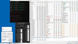
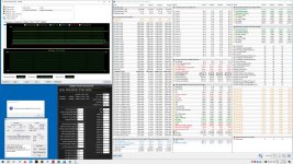
TM5 geht wie immer ohne Problem. Noch eine Stunde AIDA Kombi Test gemacht (auch nicht schlecht) Kein Prob. Leider Y Mix nach 16mins boom...
Vcore ist unter Last ~1.25V TM5, ~1.20V AIDA, ~1.16V Y Mix. 99%, dass Vcore das Problem ist, aber so eine extreme Last in Leben, nie ist.
Ich habe wieder Lust hatte zum RAM OC ;)

PS.:
TM5 geht durch eine Stufe zuerueck auch. Tx: 1.23V, VDD/Q: 1.47/1.44V Aber Y crash ~5-8 mins, wenn ich diese Spannungen nutze.
1.47/1.44, dann 1.50/1.47 liest immer ATC u. HWINFO richtig.
 

Anhänge

  • 8000_new__.jpg
    8000_new__.jpg
    716 KB · Aufrufe: 75
  • 8000_new_.jpg
    8000_new_.jpg
    763 KB · Aufrufe: 576
  • 8000_new.jpg
    8000_new.jpg
    747,3 KB · Aufrufe: 573
Chillers? Nice, which one pls? And when everything is running can you pls share a sound file from chiller? Thanks
Hailea Ultra Titan 500 (HC 300A). It will be only on CPU and RAM, MO-RA will stay on VGA and PCH.:)
I will share it. Will try it soon and clean it with a filter, so it will run for a few hours.
It was a B-stock for 380 euros. (maybe it will have a small rattling sound, but I believe I will be able to fix it myself)
 
Zuletzt bearbeitet:
Hailea Ultra Titan 500 (HC 300A). It will be only on CPU and RAM, MO-RA will stay on VGA and PCH.:)
I will share it. Will try it soon and clean it with a filter, so it will run for a few hours.
It was a B-stock for 380 euros. (maybe it will have a small rattling sound, but I believe I will be able to fix it myself)
no hurry :coffee:
 
Just tried it, 8 is the only one to go. Can it be odd number too? Maybe 7 would work too.
Most people don't know (I was in that group too) that how important WTR is.

Finally got my chiller fitting from AT, so I will be able to rebuild the loop. I think it will happen next week only, because I have to drill new holes on the case and rearrange the tubing.
It will mess up everything, but could help a lot.
Thinking on a buffer tank too, but need an elegant solution. The more the water, the less turn on for the chiller.
Whats the outcome ?
8 should still go a long way for both RRDS & WTRS
WTRS should have been 4, but at this clock its questionable :)

eh
Idk what you mean with mess up everything
Its just rearrangement, no ?
You've done it at very least once too, soo ~ i don't know.
See no issues. You got this. 🤭
Ich habe noch RRD_L/_S statt 12/8, 8/8 versucht.
Die WTR_L/_S Werte statt 24/8 --->16/4

TM5 geht wie immer ohne Problem. Noch eine Stunde AIDA Kombi Test gemacht (auch nicht schlecht) Kein Prob. Leider Y Mix nach 16mins boom...
Vcore ist unter Last ~1.25V TM5, ~1.20V AIDA, ~1.16V Y Mix. 99%, dass Vcore das Problem ist, aber so eine extreme Last in Leben, nie ist.
Ich habe wieder Lust hatte zum RAM OC ;)

PS.:
TM5 geht durch eine Stufe zuerueck auch. Tx: 1.23V, VDD/Q: 1.47/1.44V Aber Y crash ~5-8 mins, wenn ich diese Spannungen nutze.
1.47/1.44, dann 1.50/1.47 liest immer ATC u. HWINFO richtig.
Ich weiß nicht :d
1709040608273.png

Gibt es eine ODTOn_LAT Formel Änderung
Oder hast du dich verrechnet ?

X_Value - CWL - BC8 - SubChannelA & B (2) = WTR_S
Its generally strange to see ATC using (BurstChop8/Subchannel) aka 4 , yet still factoring in twice the ODTOn or PhyDly latency.
Unless its simply (-)LongDly , then why isnt formula for it (-)CAS instead. Makes no sense either.
(Ghost)Write remoted. Wr2Pre removed, BurstChop removed, ODTEnabled dly removed = raw WR 2 RD delay.
Makes no sense to my head.

1709041317547.png

Nice Powerdraw :)
Actually.
Unfortunate (V) value is the charge to reach same powertarget.
While it should be the ODT. At least in this case
But its ok~~

1.12 vs 1.15 SA is a huge change. It jumps quite a bit
CoreVID intentionally gone ?
1709042137807.png

brave_FcUIZhvDO9.png

If you are not throttling to what i see
And your memory increasing voltage requests, while your is SA dropping lower
Maybe its indeed not stable.

Lets go early suggested way and change VDD2 on "effective MC-Link" menu instead input forcing
And see if there is any way to force VDDCR_SA as VID instead of as raw input.

Vcore ist unter Last ~1.25V TM5, ~1.20V AIDA, ~1.16V Y Mix. 99%, dass Vcore das Problem ist, aber so eine extreme Last in Leben, nie ist.
.32 AC_LL cut is just not the way to approach this.
Where does CPU take VDDCR_X voltage from (_SA & _IA)
If you decide to cut input that strong.

Cutting VID on Curve is ok.
Cutting Input is not ok.
Even if telemetry faking causes CPU to adjust in reported powerdraw.
Input cutting nevertheless happens.
1709042493097.png

If it takes 1.328 DieSense.
How does it know that Cores need 1.3v chunk of it and SA needs 1.14v chunk of it.
Now what happens if you then DC_ALL telemetry fake. Result is even more skewed between request and receive. // Example
 
Gibt es eine ODTOn_LAT Formel Änderung
Oder hast du dich verrechnet ?
Einfach wollte ich es ausprobieren. Ich habe kein Problem mit 12/8 RRD u. 24/8 WTR, nun habe ich sie hier gesehen, dass viele macht das so.

Komplettes BIOS von letzte Run

Ich habe nichts gerechnet, direkt eingegeben so:

DRAM RAS# to RAS# Delay L [8]
DRAM RAS# to RAS# Delay S [8]

DRAM WRITE to READ Delay L [16]
DRAM WRITE to READ Delay S [4]

WRRD wie immer, auf auto geblieben:

tWRRD_sg [Auto]
tWRRD_dg [Auto]

Es war ein Test fuer mich auch, weil ich es dachte, dass mein Klevv kit wrong ist. Aber ich denke schon, Kit ist OK. TM5 ging immer ohne Fehler.
Es kann sein, aber ich bin nicht 100% sicher, mein ODT, RTT, RONs stoeren.

Ich nutze diese Einstellungen:

Ctl0 dqvrefup [170]
Ctl0 dqvrefdn [88]

DQ RTT WR [40 DRAM Clock]
DQ RTT NOM RD [40 DRAM Clock]
DQ RTT NOM WR [34 DRAM Clock]
DQ RTT PARK [34 DRAM Clock]
DQ RTT PARK DQS [34 DRAM Clock]
GroupA CA ODT [240 DRAM Clock]
GroupA CS ODT [0 DRAM Clock]
GroupA CK ODT [0 DRAM Clock]
GroupB CA ODT [60 DRAM Clock]
GroupB CS ODT [40 DRAM Clock]
GroupB CK ODT [40 DRAM Clock]
Pull-up Output Driver Impedance [48 DRAM Clock]
Pull-Down Output Driver Impedance [40 DRAM Clock]
DQ RTT WR [40 DRAM Clock]
DQ RTT NOM RD [40 DRAM Clock]
DQ RTT NOM WR [34 DRAM Clock]
DQ RTT PARK [34 DRAM Clock]
DQ RTT PARK DQS [34 DRAM Clock]
GroupA CA ODT [240 DRAM Clock]
GroupA CS ODT [0 DRAM Clock]
GroupA CK ODT [0 DRAM Clock]
GroupB CA ODT [60 DRAM Clock]
GroupB CS ODT [40 DRAM Clock]
GroupB CK ODT [40 DRAM Clock]
Pull-up Output Driver Impedance [40 DRAM Clock]
Pull-Down Output Driver Impedance [48 DRAM Clock]
Dimm ODT Training* [Disabled]
Max RTT_WR [ODT Off]
DIMM RON Training* [Disabled]
Read ODT Training* [Disabled]
Vddq Training [Disabled]

Ohne RTTs, ODTs geht's nicht. Sehr viele Zeit habe ich reingetan die Werte ausfinden.


System Agent ist fix 1.14V. Idle 1.12V, unter Last 1.15V

CPU System Agent Voltage [Manual Mode]
- CPU System Agent Voltage Override [1.14000]


"If you are not throttling to what i see
And your memory increasing voltage requests, while your is SA dropping lower"


Es gibt kein Trottle, ok, zu erst 400A Limit eingegeben, aber lauft es ohne irgendwelche Limit.
SA ist komisch, idle 1.12V, und wenn Y lauft staendig 1.152V


"Lets go early suggested way and change VDD2 on "effective MC-Link" menu instead input forcing
And see if there is any way to force VDDCR_SA as VID instead of as raw input."

Ich kann nur hier VDD2 eingeben, oder sorry, ich vertehe nicht etwas.

Memory Controller Voltage [1.36250]
Was neu jetzt, frueher habe es nie probiert. PMIC Voltages war immer auf auto, erste mal ausgewaehlt das Sync All PMICs. Bekommen viele untermenu. 1.25000 ausprobiert, aber gleiche wie 1.50000

PMIC Voltages [Sync All PMICs]
SPD HUB VLDO (1.8V) [1.80000]
SPD HUB VDDIO (1.0V) [1.00000]
DRAM VDD Voltage [1.50000]
DRAM VDDQ Voltage [1.47000]
DRAM VPP Voltage [1.81500]
DRAM VDD Switching Frequency [1.50000]
DRAM VDDQ Switching Frequency [1.50000]
DRAM VPP Switching Frequency [1.50000]
DRAM Current Capability [7.87500]

".32 AC_LL cut is just not the way to approach this.
Where does CPU take VDDCR_X voltage from (_SA & _IA)
If you decide to cut input that strong.

Cutting VID on Curve is ok.
Cutting Input is not ok.
Even if telemetry faking causes CPU to adjust in reported powerdraw.
Input cutting nevertheless happens."


So probiere ich irgendwie undervolt machen. Ich weiss, mit diesem silly Aktion gehe ich auf deine Nerve (sorry), aber irgendwie moechte ich Vcore so niedrig halten, wie es geht.
Ich merke es in tief, es ist Problem bei mir, das so wenig Vcore was ich mache. Wenn ich AC LL zB.: .55 einstelle und versuche ich extreme - Offset in Curve machen, irgendwie komish.
Wir nennen hier solche man, "alte floher man" ich weiss :) es ist schwer zu "kill" mein UV Style. Temperatur intressiert mich nicht, ich kann jede Zeit mein Kuehler zuerueck bauen.
30C Kuehlwasser auch nicht easy ;)
Aber du siest gut, ich steuere Vcore ueber AC LL. .050 ich schaffe schon allcore 56x ~1.20V Load Y VST. Aber das ist ~300-310W, ich habe angst, das ich diese "super" Chip kaputt mache.
Aber wenn ich .50, oder .60 AC LL eingebe, es ist geschnittet auch, nur hoeher Vcore.

Sorry, wenn ich etwas nicht verstehe.
Danke
Beitrag automatisch zusammengeführt:

Ich habe kurz Video gemacht. Statt .32 auf .35 eingestellt. So ~1.17V

Video 8000 .35 AC LL

Hier ist mein 7200, ~1.15V genug

Video 7200 ich denke .14 AC LL
 

Anhänge

  • Curve_new.jpg
    Curve_new.jpg
    169 KB · Aufrufe: 51
  • Curve_new_steps.jpg
    Curve_new_steps.jpg
    18,4 KB · Aufrufe: 52
Zuletzt bearbeitet:
I just wanted to try it out. I have no problem with 12/8 RRD and 24/8 WTR, now I've seen them here, many people do it that way.

Complete BIOS from last run

I didn't do any math, I entered it directly like this:

DRAM RAS# to RAS# Delay L [8]
DRAM RAS# to RAS# Delay S [8]

DRAM WRITE to READ Delay L [16]
DRAM WRITE to READ Delay S [4]

WRRD as always, stayed on auto:

tWRRD_sg [Auto]
tWRRD_dg [Auto]

It was a test for me too because I thought my Klevv kit was wrong. But I think so, Kit is OK. TM5 always worked without errors.
It may be, but I'm not 100% sure, my ODT, RTT, RONs are interfering.

I use these settings:

Ctl0 dqvrefup[170]
Ctl0 dqvrefdn [88]

DQ RTT WR [40 DRAM Clock]
DQ RTT NOM RD [40 DRAM Clock]
DQ RTT NOM WR [34 DRAM Clock]
DQ RTT PARK [34 DRAM Clock]
DQ RTT PARK DQS [34 DRAM Clock]
GroupA CA ODT [240 DRAM Clock]
GroupA CS ODT [0 DRAM Clock]
GroupA CK ODT [0 DRAM Clock]
GroupB CA ODT [60 DRAM Clock]
GroupB CS ODT [40 DRAM Clock]
GroupB CK ODT [40 DRAM Clock]
Pull-up Output Driver Impedance [48 DRAM Clock]
Pull-Down Output Driver Impedance [40 DRAM Clock]
DQ RTT WR [40 DRAM Clock]
DQ RTT NOM RD [40 DRAM Clock]
DQ RTT NOM WR [34 DRAM Clock]
DQ RTT PARK [34 DRAM Clock]
DQ RTT PARK DQS [34 DRAM Clock]
GroupA CA ODT [240 DRAM Clock]
GroupA CS ODT [0 DRAM Clock]
GroupA CK ODT [0 DRAM Clock]
GroupB CA ODT [60 DRAM Clock]
GroupB CS ODT [40 DRAM Clock]
GroupB CK ODT [40 DRAM Clock]
Pull-up Output Driver Impedance [40 DRAM Clock]
Pull-Down Output Driver Impedance [48 DRAM Clock]
Dimm ODT Training* [Disabled]
Max RTT_WR [ODT Off]
DIMM RON Training* [Disabled]
Read ODT Training* [Disabled]
Vddq Training [Disabled]

It doesn't work without RTTs and ODTs. I spent a lot of time finding the values.


System Agent is fixed 1.14V. Idle 1.12V, under load 1.15V

CPU System Agent Voltage [Manual Mode]
- CPU System Agent Voltage Override [1.14000]


"If you are not throttling to what I see
And your memory increasing voltage requests, while your SA is dropping lower"


There is no trouble, ok, first entered 400A limit, but it runs without any limit.
SA is strange, idle 1.12V, and when Y is constantly running 1.152V


"Lets go early suggested way and change VDD2 on "effective MC-Link" menu instead input forcing
And see if there is any way to force VDDCR_SA as VID instead of as raw input."

I can only enter VDD2 here, or sorry, I don't understand something.

Memory Controller Voltage [1.36250]
What's new now, I never tried it before. PMIC Voltages was always on auto, the first time the Sync All PMICs was selected. Get lots of submenu. Tried 1.25000 but same as 1.50000

PMIC Voltages [Sync All PMICs]
SPD HUB VLDO (1.8V) [1.80000]
SPD HUB VDDIO (1.0V) [1.00000]
DRAM VDD Voltage [1.50000]
DRAM VDDQ Voltage [1.47000]
DRAM VPP Voltage [1.81500]
DRAM VDD Switching Frequency [1.50000]
DRAM VDDQ Switching Frequency [1.50000]
DRAM VPP Switching Frequency [1.50000]
DRAM Current Capability [7.87500]

".32 AC_LL cut is just not the way to approach this.
Where does CPU take VDDCR_X voltage from (_SA & _IA)
If you decide to cut input that strong.

Cutting VID on Curve is ok.
Cutting input is not ok.
Even if telemetry faking causes CPU to adjust in reported power draw.
Input cutting still happens."


So I try to undervolt somehow. I know I'm getting on your nerves with this silly move (sorry), but somehow I want to keep Vcore as low as possible.
I notice it deep down, it's a problem for me that what I do is so little Vcore. If I set AC LL e.g.: .55 and I try to make extreme - offset in curve, somehow strange.
We call such people here, "old floher men" I know :) it's hard to "kill" my UV style. I don't care about temperature, I can put my cooler back at any time.
30C coolant isn't easy either;)
But you're good, I control Vcore via AC LL. .050 I can already manage allcore 56x ~1.20V Load Y VST. But that's ~300-310W, I'm afraid I'll break this "super" chip.
But if I enter .50 or .60 AC LL, it's cut too, just higher Vcore.

Sorry if I don't understand something.
Thanks
Beitrag automatisch zusammengeführt:

I made a short video. Set to .35 instead of .32. So ~1.17V

Video 8000 .35 AC LL

Here my 7200, ~1.15V is enough

Video 7200 I think .14 AC LL

Mind if I ask a question (and I hope English is ok lol). I am also learning the UV method by tuning the VF curve, and like you not running TVB +2 at the moment. Why is VF 11 lower (even if slightly) than VF 9 and 10 if all are 6000 ?
 
Hab jetzt mal mein SP ausgelesen. Hatte wieder Freezes. 5x
85,82,84,85,85. Ist das nun falsch oder gut?
Einmal läuft das Setup 1h40min dann error oder Freeze. Neustart, ohne was zu ändeen nach 10 min errors. Komplett Random, das ist doch schwachsin mit dem ram oc. Versuche jetzt wochenlang, diverse Spannungen. Natürlich an einer Schraube jeweils gedreht.
Vdd von 1.55-1.57
Vddq 1.5- 1.52
Tx 1.39-1.41
Imc 1.36-1.39.
Sa 1.2 könnte da mal noch tiefer gehen. Bei 1.9 mal versucht, kamen errors. Ob es wegen dem SA ist oder was anders, wer will das wissen. Bin echt ratlos... neues Bios drauf gemacht, dasselbe. Da stimmt doch was generell nicht. :(
 
Nach update auf 2002 ist die CPU verreckt :wall: . Es kam Fehler 55 . CLRCMOS gemacht / Hardreset (1 stunde Batterie raus) / Ram getauscht - Beide Bios Fehler 55 .
CPU getauscht und läuft .Gut wenn man reserve hat. Mal schauen wie lange das beim Proshop dauert.
 
Whats the outcome ?
8 should still go a long way for both RRDS & WTRS
WTRS should have been 4, but at this clock its questionable
Even 6 insta fails in Y. Only way to go is 8. At least on this foundation.
Tried WRWR_sg to 12 but it's the same.
Actually WRWR_sg on 12 with WTR_S on 8 is working, but I don't know if it helps anything.
 
Even 6 insta fails in Y. Only way to go is 8. At least on this foundation.
Tried WRWR_sg to 12 but it's the same.
Actually WRWR_sg on 12 with WTR_S on 8 is working, but I don't know if it helps anything.
WRWRsg<RDRDsg is against timing rules but is often abused within the community. I haven't ever lost stability or performance from doing it. Something to play with once one is "stable."
 
WRWRsg<RDRDsg is against timing rules but is often abused within the community. I haven't ever lost stability or performance from doing it. Something to play with once one is "stable."
Yeah, just wanted to try it as @Veii asked to try it. It didn't help.
I believe I have the limits in timings here. Maybe it doesn't play well with something else, I have no idea.
tRCDWR is also a black horse to me.
 
na endlich TM5 durch, diese scheisse.
Karhu bei 7000%. denke sieht schon besser aus.
Die Timings zeigt es falsch an bei ATC. :(
wie bringe ich die lat runter? würde gerne so 52 haben.
 

Anhänge

  • 8400c36_karhu.png
    8400c36_karhu.png
    373,5 KB · Aufrufe: 118
  • 8400c36_aida.png
    8400c36_aida.png
    429,1 KB · Aufrufe: 136
tREFI rauf und tCKE runter...Achtung, Temp. abhängig...so holst du noch ca. ns raus. Rest mit schärferem CL. Wird schwierig bei 8400...
 
Hallo zusammen.

Hat jemand vielleicht erfahrungen mit der GIGABYTE Z790 AORUS Elite X WIFI7 mainboard?
CPU und RAM OC wäre auch interesant für mich.

Ich hatte vorher ein 13600K CPU, gerade meine neue 14700K wartet auf ein neue mainboard.
Das vorherige 48er G.Skill 6800MHz kit habe ich verkauft und gerade habe ich 2 riegel von https://www.alternate.de/Team-Group...Dual-Kit-Arbeitsspeicher/html/product/1873248 (es war stark reduziert bei Alternate :) )
Eine hatte schon meine freundin ihre PC gekriegt, wo ich könnte mit ein 12400f CPU 5,1GHz takt erreichen und 6800MHz cl32 bei arbeitsspeicher in eine billig Asrock B760M PG Riptide mainboard.
(tRefi unterschied: Ich musste reduzieren wegen stabilitäte)
Ich weiss Veii erwartet mehr cycles und dazu vst&vt3 auch, aber diese PC muss nicht "NASA stabil" sein, wie zebra_hun sagt es immer :)
Ich finde das ergebniss schon schön von dieses bundel.
 

Anhänge

  • 6800 cl32 T-force.jpg
    6800 cl32 T-force.jpg
    539 KB · Aufrufe: 68
  • boahh.JPG
    boahh.JPG
    44,6 KB · Aufrufe: 77
  • A-Die 2.jpg
    A-Die 2.jpg
    345,4 KB · Aufrufe: 69
na endlich TM5 durch, diese scheisse.
Karhu bei 7000%. denke sieht schon besser aus.
Die Timings zeigt es falsch an bei ATC. :(
wie bringe ich die lat runter? würde gerne so 52 haben.
tRAS ist zu hoch. Muesstest du 61, 65, 69 probieren.
Beitrag automatisch zusammengeführt:

Hello everyone.

Does anyone have any experience with the GIGABYTE Z790 AORUS Elite X WIFI7 mainboard?
CPU and RAM OC would also be interesting for me.

I previously had a 13600K CPU, my new 14700K is currently waiting for a new motherboard.
I sold the previous 48 G.Skill 6800MHz kit and I currently have 2 bars from https://www.alternate.de/Team-Group/DIMM-32-GB-DDR5-7200-(2x-16-GB)- Dual kit memory/html/product/1873248 (it was heavily discounted at Alternate :) )
My friend had already gotten her PC, where I could achieve a clock speed of 5.1GHz with a 12400f CPU and 6800MHz cl32 with RAM in a cheap Asrock B760M PG Riptide motherboard.
(tRefi difference: I had to reduce because of stability)
I know Veii expects more cycles and vst&vt3 too, but this PC doesn't have to be "NASA stable", as zebra_hun always says:)
I think the results of this bundle are beautiful.
WTRL=2xRRDL schauet schoen!

Um 6800 RFC/RFCpb sollten niedriger tun. Von 480/390, 512/416 kannst du waehlen.

@ 6800 tCKE 17, tCPDED 17, tXP 26.
 
Zuletzt bearbeitet:
Ok also, einerseits tras tiefer, zb 84 oder noch tiefer, wenns natürlich läuft.
Oder
Tcke runter, trefi rauf sprich 26xxx oder sogar 131xx?
 
Mach zuerst das tRas...dann testen...dann tREFI 131xxx...aber kühlen musst du's können.
Dann testen...dann tCKE und wieder testen
 
tRAS ist zu hoch. Muesstest du 61, 65, 69 probieren.
Beitrag automatisch zusammengeführt:


WTRL=2xRRDL schauet schoen!

Um 6800 RFC/RFCpb sollten niedriger tun. Von 480/390, 512/416 kannst du waehlen.

@ 6800 tCKE 17, tCPDED 17, tXP 26.
Hallo

CarSalesman


tWTR_S und L sind 4 und 16 eingestellt in bios. ATC zeigt anderes.
tRFC wollte ich schon reduzieren, bald mache ich, wenn ich mehr zeit habe. :) Es war noch auto.
Wie ich habe das gemerkt, was wichtig ist bei ddr5 ist der tREFI(bringt bei latency sehr viel) und tWRRD_sg und_dg, die beide bringt viel extra geschwindigkeit (nicht bei aida64 bench ... in game) ich versuche immer in niedrigste wert halten.
tCKE kann ich probieren, aber lohnt sich? Wie hast du das 17er wert ausgerechnet?

Danke dir eigentlich das tip.
Ich bin immer noch noob bei ddr5 :d
ATC addiert immer 4 zu WTR's.

tCKE und tCPDED muessen mindestens 5 ns sein; tXP mindestens 7.5 ns. Sie haengen von der Frequenz ab.

5/(2000/6800) ≈ 17
7.5/(2000/6800) ≈ 26
 
Zuletzt bearbeitet:
I took some time to work on the deltas and BIOS versions. I had many retraining problems in Cold Boot, sometimes with the PSU off or sometimes in Stand By, after spending many hours, YC would fail directly. The beta version 9901 (based on the 1202) was much better for me.

This would be the foundation, to grow to where my IMC is capable. I managed to boot 8600 but it is not the goal nor do I think I can sustain it with my cooling.

My configuration data for 8000-38-48-48-48-64.
VDD 1.45 / VDD2 1.35
VDDQ_mem 1.39 / VDDQ 1.19
SA 1.14
TWR 24/tRRDL/S 8-8 and WTRL/S 24-8
RONs 48-40/40-48 - CTL0 DQVrefUp set and VDDQ Training / RON Disabled
Core and Cache Current Limit 400A (This allows me to reach 5.6 and 5.7 in the best cores). It is not ideal, so I think it is advisable to leave everything unlimited but the truth is, for the use I give it in my case, when I am going to run a test with so much power draw. I saw the reference that Veii put about the man who has the greensticks and a great delta for 8400 with VDDQM 1.41 and VDDQ2 1.185v, with SA 1.18, which limited his Current Limit to 346A, you can see behind that HWInfo shows 253W the maximum, having Unlimited PL1/2.
Oh, lastly, leave the RTTs on Auto and I set RxDfe to On. I used to enable it, but I don't know if it's okay in this semi-auto configuration.
8000C38 Foundation BIOS 9901.jpg
I have some questions left, since I previously ran 8266 without delta, with high TX, and with false stability.

Having these values as a foundation. The key question is, how do voltages scale?

Some are linear and others are not. If, for example, I go to 8200 as the next step, what increase should the data lines and VDD2 have?

Or for example do VDDQ-VDDQ scale? In case I take as a reference the one who made the POC of 8400 with the greens at 1.41 from VDDQM, although they are greens, and I am at 1.39... It doesn't have much relation. Should I increase it by, for example, 0.25%? i.e. 1.43 VDDQ_mem for 1.23VDDQCPU?

And regarding SA? I understand that it is linear to the SVID... and for high speeds I noticed that I need more voltage, perhaps it is an error, but in 8400 if I go below 1.2 I have instantaneous YC errors, perhaps the deltas are not well defined.

At least to learn, I think a good real objective would be if I could run 8400 with loose timings or 8200 with better timings. I think my CPU could do it with P114 E88 MC 83 but I don't know if my 8000 H16A memories could do it, because the H24M are very optimized, I mean 8400 at 1.45? They are 400MHz more at the same voltage.
Ahh maybe a sidenote
There are several ICCMAX.

Ring has own
IA supply has an own
GT has an own
And i dont know about VDDQ ICCMAX, but it likely can stay maxed. Although i dont how to track it really.
I think ASUS Worktool doesnt list this - maybe , been some time now.

Thermal throttling is not bad , really is not.
Its soo much better than an emergency powerlimit.
PT1 / PPT is a low powerlimit, its basically a PSU limiter & used as TDP limiter.
PowerTarget? 2 is the same limiter but the short side of Wattage. As wattage/sec is a very silly "Title"
Wattage is a durational powerlimit. Electrical limiters are softer and per-core thermal limiters are much better than this. *
* as long as you don't reach TJ-MAX limiters. Those are emergency limiters too.

Wattage also doesnt equally translate to heat.
Soo its the least split in short and long durations.
ICCMAX is more of a transient and substrate limiter than it is anything else.

Its good to have it set, but if you have no margins, it absolutely will ruin your higher clock and usable raw performance.
Soo i see why it is at 510A on OC boards, even if this definitely does damage CPUs.
We are just an exception and a little % of the actual userbase.
I don't like myself that its silly silly high. Even 400A is silly high but Intel™ says its fine within some reasons.
Hi @Veii! I didn't know about all the ICCMAX lines, in the end I ended up leaving IVR VDDQ ICCMAX in Auto, ICCMAX Unlimited (so that it goes above the os 511A) disabled, and Core/Cache Current in 400, I think it is the safest for so many tests with YCruncher
Whats the V/F curve of your current 14th gen sample.
That's my V/F Curve :-)
VF Curve.jpg
For the community, this is my BIOS config file
[2024/02/28 22:39:16]
Ai Overclock Tuner [Manual]
BCLK Frequency [100.0000]
PCIE Frequency [100.0000]
Intel(R) Adaptive Boost Technology [Auto]
ASUS MultiCore Enhancement [Enabled – Remove All limits]
SVID Behavior [Trained]
BCLK Frequency : DRAM Frequency Ratio [Auto]
Memory Controller : DRAM Frequency Ratio [Auto]
DRAM Frequency [DDR5-8000MHz]
DIMM Flex [Disabled]
Performance Core Ratio [Auto]
Performance Core0 Specific Ratio Limit [Auto]
Performance Core0 specific Voltage [Auto]
Performance Core1 Specific Ratio Limit [Auto]
Performance Core1 specific Voltage [Auto]
Performance Core2 Specific Ratio Limit [Auto]
Performance Core2 specific Voltage [Auto]
Performance Core3 Specific Ratio Limit [Auto]
Performance Core3 specific Voltage [Auto]
*Performance Core4 Specific Ratio Limit [Auto]
Performance Core4 specific Voltage [Auto]
*Performance Core5 Specific Ratio Limit [Auto]
Performance Core5 specific Voltage [Auto]
Performance Core6 Specific Ratio Limit [Auto]
Performance Core6 specific Voltage [Auto]
Performance Core7 Specific Ratio Limit [Auto]
Performance Core7 specific Voltage [Auto]
Efficient Core Ratio [Auto]
Efficient Core Group0 Specific Ratio Limit [Auto]
Efficient Core Group0 specific Voltage [Auto]
Efficient Core Group1 Specific Ratio Limit [Auto]
Efficient Core Group1 specific Voltage [Auto]
Efficient Core Group2 Specific Ratio Limit [Auto]
Efficient Core Group2 specific Voltage [Auto]
Efficient Core Group3 Specific Ratio Limit [Auto]
Efficient Core Group3 specific Voltage [Auto]
AVX2 [Enabled]
AVX2 Ratio Offset to per-core Ratio Limit [User Specify]
AVX2 Ratio Offset [0]
AVX2 Voltage Guardband Scale Factor [Auto]
Maximus Tweak [Mode 1]
DRAM CAS# Latency [38]
DRAM RAS# to CAS# Delay Read [48]
DRAM RAS# to CAS# Delay Write [48]
DRAM RAS# PRE Time [48]
DRAM RAS# ACT Time [64]
DRAM Command Rate [2N]
DRAM RAS# to RAS# Delay L [8]
DRAM RAS# to RAS# Delay S [8]
DRAM REF Cycle Time 2 [512]
DRAM REF Cycle Time Same Bank [416]
DRAM Refresh Interval [65535]
DRAM WRITE Recovery Time [24]
DRAM READ to PRE Time [12]
DRAM FOUR ACT WIN Time [32]
DRAM WRITE to READ Delay L [24]
DRAM WRITE to READ Delay S [8]
DRAM CKE Minimum Pulse Width [20]
DRAM Write Latency [36]
Ctl0 dqvrefup [170]
Ctl0 dqvrefdn [88]
Ctl0 dqodtvrefup [Auto]
Ctl0 dqodtvrefdn [Auto]
Ctl1 cmdvrefup [Auto]
Ctl1 ctlvrefup [Auto]
Ctl1 clkvrefup [Auto]
Ctl1 ckecsvrefup [Auto]
Ctl2 cmdvrefdn [Auto]
Ctl2 ctlvrefdn [Auto]
Ctl2 clkvrefdn [Auto]
Read Equalization RxEq Start Sign [-]
Read Equalization RxEq Start [Auto]
Read Equalization RxEq Stop Sign [-]
Read Equalization RxEq Stop [Auto]
ODT_READ_DURATION [Auto]
ODT_READ_DELAY [Auto]
ODT_WRITE_DURATION [Auto]
ODT_WRITE_DELAY [Auto]
DQ RTT WR [Auto]
DQ RTT NOM RD [Auto]
DQ RTT NOM WR [Auto]
DQ RTT PARK [Auto]
DQ RTT PARK DQS [Auto]
GroupA CA ODT [Auto]
GroupA CS ODT [Auto]
GroupA CK ODT [Auto]
GroupB CA ODT [Auto]
GroupB CS ODT [Auto]
GroupB CK ODT [Auto]
Pull-up Output Driver Impedance [48 DRAM Clock]
Pull-Down Output Driver Impedance [40 DRAM Clock]
DQ RTT WR [Auto]
DQ RTT NOM RD [Auto]
DQ RTT NOM WR [Auto]
DQ RTT PARK [Auto]
DQ RTT PARK DQS [Auto]
GroupA CA ODT [Auto]
GroupA CS ODT [Auto]
GroupA CK ODT [Auto]
GroupB CA ODT [Auto]
GroupB CS ODT [Auto]
GroupB CK ODT [Auto]
Pull-up Output Driver Impedance [40 DRAM Clock]
Pull-Down Output Driver Impedance [48 DRAM Clock]
Round Trip Latency Init Value MC0 CHA [Auto]
Round Trip Latency Max Value MC0 CHA [Auto]
Round Trip Latency Offset Value Mode Sign MC0 CHA [-]
Round Trip Latency Offset Value MC0 CHA [Auto]
Round Trip Latency Init Value MC0 CHB [Auto]
Round Trip Latency Max Value MC0 CHB [Auto]
Round Trip Latency Offset Value Mode Sign MC0 CHB [-]
Round Trip Latency Offset Value MC0 CHB [Auto]
Round Trip Latency Init Value MC1 CHA [Auto]
Round Trip Latency Max Value MC1 CHA [Auto]
Round Trip Latency Offset Value Mode Sign MC1 CHA [-]
Round Trip Latency Offset Value MC1 CHA [Auto]
Round Trip Latency Init Value MC1 CHB [Auto]
Round Trip Latency Max Value MC1 CHB [Auto]
Round Trip Latency Offset Value Mode Sign MC1 CHB [-]
Round Trip Latency Offset Value MC1 CHB [Auto]
Round Trip Latency MC0 CHA R0 [Auto]
Round Trip Latency MC0 CHA R1 [Auto]
Round Trip Latency MC0 CHA R2 [0]
Round Trip Latency MC0 CHA R3 [0]
Round Trip Latency MC0 CHA R4 [0]
Round Trip Latency MC0 CHA R5 [0]
Round Trip Latency MC0 CHA R6 [0]
Round Trip Latency MC0 CHA R7 [0]
Round Trip Latency MC0 CHB R0 [Auto]
Round Trip Latency MC0 CHB R1 [Auto]
Round Trip Latency MC0 CHB R2 [0]
Round Trip Latency MC0 CHB R3 [0]
Round Trip Latency MC0 CHB R4 [0]
Round Trip Latency MC0 CHB R5 [0]
Round Trip Latency MC0 CHB R6 [0]
Round Trip Latency MC0 CHB R7 [0]
Round Trip Latency MC1 CHA R0 [Auto]
Round Trip Latency MC1 CHA R1 [Auto]
Round Trip Latency MC1 CHA R2 [0]
Round Trip Latency MC1 CHA R3 [0]
Round Trip Latency MC1 CHA R4 [0]
Round Trip Latency MC1 CHA R5 [0]
Round Trip Latency MC1 CHA R6 [0]
Round Trip Latency MC1 CHA R7 [0]
Round Trip Latency MC1 CHB R0 [Auto]
Round Trip Latency MC1 CHB R1 [Auto]
Round Trip Latency MC1 CHB R2 [0]
Round Trip Latency MC1 CHB R3 [0]
Round Trip Latency MC1 CHB R4 [0]
Round Trip Latency MC1 CHB R5 [0]
Round Trip Latency MC1 CHB R6 [0]
Round Trip Latency MC1 CHB R7 [0]
Early Command Training [Auto]
SenseAmp Offset Training [Auto]
Early ReadMPR Timing Centering 2D [Auto]
Read MPR Training [Auto]
Receive Enable Training [Auto]
Jedec Write Leveling [Auto]
Early Write Time Centering 2D [Auto]
Early Read Time Centering 2D [Auto]
Write Timing Centering 1D [Auto]
Write Voltage Centering 1D [Auto]
Read Timing Centering 1D [Auto]
Read Timing Centering with JR [Auto]
Dimm ODT Training* [Auto]
Max RTT_WR [ODT Off]
DIMM RON Training* [Disabled]
Write Drive Strength/Equalization 2D* [Auto]
Write Slew Rate Training* [Auto]
Read ODT Training* [Auto]
Comp Optimization Training [Auto]
Read Equalization Training* [Auto]
Read Amplifier Training* [Auto]
Write Timing Centering 2D [Auto]
Read Timing Centering 2D [Auto]
Command Voltage Centering [Auto]
Early Command Voltage Centering [Auto]
Write Voltage Centering 2D [Auto]
Read Voltage Centering 2D [Auto]
Late Command Training [Auto]
Round Trip Latency [Auto]
Turn Around Timing Training [Auto]
CMD CTL CLK Slew Rate [Auto]
CMD/CTL DS & E 2D [Auto]
Read Voltage Centering 1D [Auto]
TxDqTCO Comp Training* [Auto]
ClkTCO Comp Training* [Auto]
TxDqsTCO Comp Training* [Auto]
VccDLL Bypass Training [Auto]
CMD/CTL Drive Strength Up/Dn 2D [Auto]
DIMM CA ODT Training [Auto]
PanicVttDnLp Training* [Auto]
Read Vref Decap Training* [Auto]
Vddq Training [Disabled]
Duty Cycle Correction Training [Auto]
Periodic DCC [Auto]
Rank Margin Tool Per Bit [Auto]
DIMM DFE Training [Auto]
EARLY DIMM DFE Training [Auto]
Tx Dqs Dcc Training [Auto]
DRAM DCA Training [Auto]
Write Driver Strength Training [Auto]
Rank Margin Tool [Auto]
Memory Test [Auto]
DIMM SPD Alias Test [Auto]
Receive Enable Centering 1D [Auto]
Retrain Margin Check [Auto]
Write Drive Strength Up/Dn independently [Auto]
LPDDR DqDqs Re-Training [Auto]
Margin Check Limit [Disabled]
tRDRD_sg_Training [Auto]
tRDRD_sg_Runtime [16]
tRDRD_dg_Training [Auto]
tRDRD_dg_Runtime [8]
tRDWR_sg [20]
tRDWR_dg [20]
tWRWR_sg [16]
tWRWR_dg [8]
tWRRD_sg [Auto]
tWRRD_dg [Auto]
tRDRD_dr [0]
tRDRD_dd [0]
tRDWR_dr [0]
tRDWR_dd [0]
tWRWR_dr [0]
tWRWR_dd [0]
tWRRD_dr [0]
tWRRD_dd [0]
tRPRE [Auto]
tWPRE [Auto]
tWPOST [Auto]
tWRPRE [Auto]
tPRPDEN [Auto]
tRDPDEN [Auto]
tWRPDEN [Auto]
tCPDED [20]
tREFIX9 [Auto]
Ref Interval [Auto]
tXPDLL [Auto]
tXP [30]
tPPD [2]
tCCD_L_tDLLK [Auto]
tZQCAL [Auto]
tZQCS [Auto]
OREF_RI [Auto]
Refresh Watermarks [High]
Refresh Hp Wm [Auto]
Refresh Panic Wm [Auto]
Refresh Abr Release [Auto]
tXSDLL [2560]
tZQOPER [Auto]
tMOD [Auto]
CounttREFIWhileRefEn [Auto]
HPRefOnMRS [Auto]
SRX Ref Debits [Auto]
RAISE BLK WAIT [Auto]
Ref Stagger En [Auto]
Ref Stagger Mode [Auto]
Disable Stolen Refresh [Auto]
En Ref Type Display [Auto]
Trefipulse Stagger Disable [Auto]
tRPab ext [Auto]
derating ext [Auto]
Allow 2cyc B2B LPDDR [Auto]
tCSH [Auto]
tCSL [Auto]
powerdown Enable [Auto]
idle length [Auto]
raise cke after exit latency [Auto]
powerdown latency [Auto]
powerdown length [Auto]
selfrefresh latency [Auto]
selfrefresh length [Auto]
ckevalid length [Auto]
ckevalid enable [Auto]
idle enable [Auto]
selfrefresh enable [Auto]
Address mirror [Auto]
no gear4 param divide [Auto]
x8 device [Auto]
no gear2 param divide [Auto]
ddr 1dpc split ranks on subch [Auto]
write0 enable [Auto]
MultiCycCmd [Auto]
WCKDiffLowInIdle [Auto]
PBR Disable [Auto]
PBR OOO Dis [Auto]
PBR Disable on hot [Auto]
PBR Exit on Idle Cnt [Auto]
tXSR [551]
Dec tCWL [Auto]
Add tCWL [Auto]
Add 1Qclk delay [Auto]
MRC Fast Boot [Disabled]
MCH Full Check [Auto]
Mem Over Clock Fail Count [2]
Training Profile [Auto]
RxDfe [Enabled]
Mrc Training Loop Count [Auto]
DRAM CLK Period [Auto]
Dll_bwsel [Auto]
Controller 0, Channel 0 Control [Enabled]
Controller 0, Channel 1 Control [Enabled]
Controller 1, Channel 0 Control [Enabled]
Controller 1, Channel 1 Control [Enabled]
MC_Vref0 [Auto]
MC_Vref1 [Auto]
MC_Vref2 [Auto]
Fine Granularity Refresh mode [Enabled]
SDRAM Density Per Die [Auto]
SDRAM Banks Per Bank Group [Auto]
SDRAM Bank Groups [Auto]
Dynamic Memory Boost [Disabled]
Realtime Memory Frequency [Disabled]
SA GV [Disabled]
Voltage Monitor [Die Sense]
VRM Initialization Check [Enabled]
CPU Input Voltage Load-line Calibration [Level 2]
CPU Load-line Calibration [Level 4:Recommended for OC]
Synch ACDC Loadline with VRM Loadline [Disabled]
CPU Current Capability [120%]
CPU Current Reporting [Auto]
Core Voltage Suspension [Auto]
CPU VRM Switching Frequency [Auto]
VRM Spread Spectrum [Disabled]
CPU Power Duty Control [T.Probe]
CPU Power Phase Control [Extreme]
CPU Power Thermal Control [125]
CPU Core/Cache Boot Voltage [Auto]
CPU Input Boot Voltage [Auto]
PLL Termination Boot Voltage [Auto]
CPU Standby Boot Voltage [Auto]
Memory Controller Boot Voltage [Auto]
CPU Core Auto Voltage Cap [Auto]
CPU Input Auto Voltage Cap [Auto]
Memory Controller Auto Voltage Cap [Auto]
Maximum CPU Core Temperature [Auto]
Fast Throttle Threshold [Auto]
Package Temperature Threshold [Auto]
Regulate Frequency by above Threshold [Auto]
IVR Transmitter VDDQ ICCMAX [Auto]
Unlimited ICCMAX [Disabled]
CPU Core/Cache Current Limit Max. [400.00]
Long Duration Package Power Limit [Auto]
Package Power Time Window [Auto]
Short Duration Package Power Limit [Auto]
Dual Tau Boost [Disabled]
IA AC Load Line [Auto]
IA DC Load Line [Auto]
IA CEP [Auto]
SA CEP [Auto]
IA SoC Iccmax Reactive Protector [Auto]
Inverse Temperature Dependency Throttle [Auto]
IA VR Voltage Limit [1550]
CPU SVID Support [Auto]
Cache Dynamic OC Switcher [Auto]
TVB Voltage Optimizations [Auto]
Enhanced TVB [Auto]
Overclocking TVB [Auto]
Overclocking TVB Global Temperature Offset Sign [+]
Overclocking TVB Global Temperature Offset Value [Auto]
Offset Mode Sign 1 [+]
V/F Point 1 Offset [Auto]
Offset Mode Sign 2 [+]
V/F Point 2 Offset [Auto]
Offset Mode Sign 3 [+]
V/F Point 3 Offset [Auto]
Offset Mode Sign 4 [+]
V/F Point 4 Offset [Auto]
Offset Mode Sign 5 [+]
V/F Point 5 Offset [Auto]
Offset Mode Sign 6 [+]
V/F Point 6 Offset [Auto]
Offset Mode Sign 7 [+]
V/F Point 7 Offset [Auto]
Offset Mode Sign 8 [+]
V/F Point 8 Offset [Auto]
Offset Mode Sign 9 [+]
V/F Point 9 Offset [Auto]
Offset Mode Sign 10 [+]
V/F Point 10 Offset [Auto]
Offset Mode Sign 11 [+]
V/F Point 11 Offset [Auto]
Initial BCLK Frequency [Auto]
Runtime BCLK OC [Auto]
BCLK Amplitude [Auto]
BCLK Slew Rate [Auto]
BCLK Spread Spectrum [Disabled]
Initial PCIE Frequency [Auto]
PCIE/DMI Amplitude [Auto]
PCIE/DMI Slew Rate [Auto]
PCIE/DMI Spread Spectrum [Disabled]
Cold Boot PCIE Frequency [Auto]
Realtime Memory Timing [Enabled]
SPD Write Disable [TRUE]
PVD Ratio Threshold [Auto]
SA PLL Frequency Override [Auto]
BCLK TSC HW Fixup [Enabled]
Core Ratio Extension Mode [Disabled]
FLL OC mode [Auto]
UnderVolt Protection [Disabled]
Switch Microcode [Current Microcode]
Xtreme Tweaking [Disabled]
Core PLL Voltage [Auto]
GT PLL Voltage [Auto]
Ring PLL Voltage [Auto]
System Agent PLL Voltage [Auto]
Memory Controller PLL Voltage [Auto]
Efficient-core PLL Voltage [Auto]
CPU 1.8V Small Rail [Auto]
PLL Termination Voltage [Auto]
CPU Standby Voltage [Auto]
PCH 1.05V Voltage [Auto]
PCH 0.82V Voltage [Auto]
CPU Input Voltage Reset Voltage [Auto]
Eventual CPU Input Voltage [Auto]
Eventual Memory Controller Voltage [Auto]
Package Temperature Threshold [Auto]
Regulate Frequency by above Threshold [Auto]
Cooler Efficiency Customize [Keep Training]
Cooler Re-evaluation Algorithm [Normal]
Optimism Scale [100]
Ring Down Bin [Auto]
Min. CPU Cache Ratio [Auto]
Max. CPU Cache Ratio [Auto]
BCLK Aware Adaptive Voltage [Auto]
Actual VRM Core Voltage [Auto]
Global Core SVID Voltage [Auto]
Cache SVID Voltage [Auto]
CPU L2 Voltage [Adaptive Mode]
- Offset Mode Sign [+]
- Additional Turbo Mode CPU L2 Voltage [Auto]
- Offset Voltage [0.05000]
CPU System Agent Voltage [Manual Mode]
- CPU System Agent Voltage Override [1.14000]
CPU Input Voltage [Auto]
High DRAM Voltage Mode [Enabled]
DRAM VDD Voltage [1.45000]
DRAM VDDQ Voltage [1.39000]
IVR Transmitter VDDQ Voltage [1.19000]
Memory Controller Voltage [1.35000]
MC Voltage Calculation Voltage Base [Auto]
VDD Calculation Voltage Base [Auto]
PMIC Voltages [Sync All PMICs]
SPD HUB VLDO (1.8V) [1.80000]
SPD HUB VDDIO (1.0V) [1.00000]
DRAM VDD Voltage [1.45000]
DRAM VDDQ Voltage [1.39000]
DRAM VPP Voltage [1.82000]
DRAM VDD Switching Frequency [1.50000]
DRAM VDDQ Switching Frequency [1.50000]
DRAM VPP Switching Frequency [1.50000]
DRAM Current Capability [7.87500]
PCI Express Native Power Management [Enabled]
Native ASPM [Disabled]
DMI Link ASPM Control [Disabled]
ASPM [Auto]
L1 Substates [Disabled]
DMI ASPM [Disabled]
DMI Gen3 ASPM [Disabled]
PEG - ASPM [Disabled]
PCI Express Clock Gating [Enabled]
Hardware Prefetcher [Enabled]
Adjacent Cache Line Prefetch [Enabled]
Intel (VMX) Virtualization Technology [Disabled]
Per P-Core Control [Disabled]
Per E-Core Control [Disabled]
Active Performance Cores [All]
Active Efficient Cores [All]
Hyper-Threading [Enabled]
Hyper-Threading of Core 0 [Enabled]
Hyper-Threading of Core 1 [Enabled]
Hyper-Threading of Core 2 [Enabled]
Hyper-Threading of Core 3 [Enabled]
Hyper-Threading of Core 4 [Enabled]
Hyper-Threading of Core 5 [Enabled]
Hyper-Threading of Core 6 [Enabled]
Hyper-Threading of Core 7 [Enabled]
Total Memory Encryption [Disabled]
Legacy Game Compatibility Mode [Disabled]
Boot performance mode [Auto]
Intel(R) SpeedStep(tm) [Enabled]
Intel(R) Speed Shift Technology [Enabled]
Intel(R) Turbo Boost Max Technology 3.0 [Enabled]
Turbo Mode [Enabled]
Acoustic Noise Mitigation [Disabled]
CPU C-states [Auto]
Thermal Monitor [Enabled]
Dual Tau Boost [Disabled]
VT-d [Disabled]
Memory Remap [Enabled]
Enable VMD controller [Enabled]
Map PCIE Storage under VMD [Disabled]
Map SATA Controller under VMD [Disabled]
M.2_2 Link Speed [Auto]
PCIEX16(G5)_1 Link Speed [Auto]
M.2_1 Link Speed [Auto]
PCIEX4(G4)_1 Link Speed [Auto]
PCIEX4(G4)_2 Link Speed [Auto]
M.2_3 Link Speed [Auto]
DIMM.2_1 Link Speed [Auto]
DIMM.2_2 Link Speed [Auto]
SATA Controller(s) [Enabled]
Aggressive LPM Support [Disabled]
SMART Self Test [Enabled]
M.2_3 [Enabled]
M.2_3 Hot Plug [Disabled]
SATA6G_1 [Enabled]
SATA6G_1 Hot Plug [Disabled]
SATA6G_2 [Enabled]
SATA6G_2 Hot Plug [Disabled]
SATA6G_3 [Enabled]
SATA6G_3 Hot Plug [Disabled]
SATA6G_4 [Enabled]
SATA6G_4 Hot Plug [Disabled]
PTT [Enable]
Intel(R) Dynamic Tuning Technology [Disabled]
PCIE Tunneling over USB4 [Enabled]
Discrete Thunderbolt(TM) Support [Disabled]
Security Device Support [Enable]
SHA256 PCR Bank [Enabled]
Pending operation [None]
Platform Hierarchy [Enabled]
Storage Hierarchy [Enabled]
Endorsement Hierarchy [Enabled]
Physical Presence Spec Version [1.3]
Disable Block Sid [Disabled]
USB Host Controller Support [Disabled]
Password protection of Runtime Variables [Enable]
Above 4G Decoding [Enabled]
Resize BAR Support [Enabled]
SR-IOV Support [Disabled]
Legacy USB Support [Enabled]
XHCI Hand-off [Enabled]
Lexar microSD RDR 0815 [Auto]
U10G_1 [Enabled]
U5G_E5 [Enabled]
U5G_E6 [Enabled]
U5G_E7 [Enabled]
U5G_E8 [Enabled]
U20G_C3 [Enabled]
U10G_5 [Enabled]
U10G_6 [Enabled]
U10G_7 [Enabled]
U10G_8 [Enabled]
U20G_C9 [Enabled]
USB11 [Enabled]
USB12 [Enabled]
U32G1_E1 [Enabled]
U32G1_E2 [Enabled]
U32G1_E3 [Enabled]
U32G1_E4 [Enabled]
Network Stack [Disabled]
Device [N/A]
Restore AC Power Loss [Power Off]
Max Power Saving [Disabled]
ErP Ready [Disabled]
Power On By PCI-E [Disabled]
Power On By RTC [Disabled]
PCIe Bandwidth Bifurcation Configuration [Auto]
USB Audio [Enabled]
Intel LAN [Enabled]
USB power delivery in Soft Off state (S5) [Enabled]
Wi-Fi Controller [Enabled]
Bluetooth Controller [Enabled]
When system is in working state [All On]
Q-Code LED Function [Auto]
When system is in sleep, hibernate or soft off states [All On]
M.2_3 Configuration [Auto]
CPU PCIE Configuration Mode [Auto]
ASMedia USB 3.2 Controller_U5G_E12 [Enabled]
ASMedia USB 3.2 Controller_U5G_E34 [Enabled]
GNA Device [Disabled]
Alteration Mode Switch [PCIE Link Speed]
CPU Temperature [Monitor]
CPU Package Temperature [Monitor]
MotherBoard Temperature [Monitor]
VRM Temperature [Monitor]
Chipset Temperature [Monitor]
T_Sensor Temperature [Monitor]
DIMM.2 Sensor 1 Temperature [Monitor]
DIMM.2 Sensor 2 Temperature [Monitor]
Water In T Sensor Temperature [Monitor]
Water Out T Sensor Temperature [Monitor]
DIMM Thermistor Temperature [Monitor]
DIMM A1 Temperature [Monitor]
DIMM B1 Temperature [Monitor]
CPU Fan Speed [Monitor]
CPU Optional Fan Speed [Monitor]
Chassis Fan 1 Speed [Monitor]
Chassis Fan 2 Speed [Monitor]
Extra Flow Fan Speed [Monitor]
Water Pump+ Speed [Monitor]
AIO Pump Speed [Monitor]
Flow Rate [Monitor]
CPU Core Voltage [Monitor]
12V Voltage [Monitor]
5V Voltage [Monitor]
3.3V Voltage [Monitor]
Memory Controller Voltage [Monitor]
CPU Fan Q-Fan Control [PWM Mode]
CPU Fan Profile [Manual]
CPU Fan Q-Fan Source [CPU]
CPU Fan Step Up [Level 0]
CPU Fan Step Down [Level 0]
CPU Fan Speed Low Limit [200 RPM]
CPU Fan Point4 Temperature [60]
CPU Fan Point4 Duty Cycle (%) [100]
CPU Fan Point3 Temperature [47]
CPU Fan Point3 Duty Cycle (%) [83]
CPU Fan Point2 Temperature [34]
CPU Fan Point2 Duty Cycle (%) [63]
CPU Fan Point1 Temperature [18]
CPU Fan Point1 Duty Cycle (%) [39]
Chassis Fan 1 Q-Fan Control [Auto Detect]
Chassis Fan 1 Profile [Manual]
Chassis Fan 1 Q-Fan Source [CPU]
Chassis Fan 1 Step Up [Level 0]
Chassis Fan 1 Step Down [Level 0]
Chassis Fan 1 Speed Low Limit [200 RPM]
Chassis Fan 1 Point4 Temperature [70]
Chassis Fan 1 Point4 Duty Cycle (%) [100]
Chassis Fan 1 Point3 Temperature [65]
Chassis Fan 1 Point3 Duty Cycle (%) [100]
Chassis Fan 1 Point2 Temperature [45]
Chassis Fan 1 Point2 Duty Cycle (%) [100]
Chassis Fan 1 Point1 Temperature [21]
Chassis Fan 1 Point1 Duty Cycle (%) [100]
Chassis Fan 2 Q-Fan Control [Auto Detect]
Chassis Fan 2 Profile [Manual]
Chassis Fan 2 Q-Fan Source [CPU]
Chassis Fan 2 Step Up [Level 0]
Chassis Fan 2 Step Down [Level 0]
Chassis Fan 2 Speed Low Limit [200 RPM]
Chassis Fan 2 Point4 Temperature [70]
Chassis Fan 2 Point4 Duty Cycle (%) [100]
Chassis Fan 2 Point3 Temperature [65]
Chassis Fan 2 Point3 Duty Cycle (%) [100]
Chassis Fan 2 Point2 Temperature [45]
Chassis Fan 2 Point2 Duty Cycle (%) [100]
Chassis Fan 2 Point1 Temperature [28]
Chassis Fan 2 Point1 Duty Cycle (%) [100]
Extra Flow Fan Q-Fan Control [DC Mode]
Extra Flow Fan Profile [Manual]
Extra Flow Fan Q-Fan Source [DIMM Thermistor]
Extra Flow Fan Step Up [Level 0]
Extra Flow Fan Step Down [Level 0]
Extra Flow Fan Speed Low Limit [Ignore]
Extra Flow Fan Point4 Temperature [81]
Extra Flow Fan Point4 Duty Cycle (%) [0]
Extra Flow Fan Point3 Temperature [60]
Extra Flow Fan Point3 Duty Cycle (%) [0]
Extra Flow Fan Point2 Temperature [45]
Extra Flow Fan Point2 Duty Cycle (%) [0]
Extra Flow Fan Point1 Temperature [20]
Extra Flow Fan Point1 Duty Cycle (%) [0]
Allow Fan Stop [Disabled]
Water Pump+ Q-Fan Control [Auto Detect]
Water Pump+ Profile [Full Speed]
AIO Pump Q-Fan Control [Auto Detect]
AIO Pump Profile [Full Speed]
CPU Temperature LED Switch [Enabled]
Launch CSM [Disabled]
OS Type [Windows UEFI mode]
Secure Boot Mode [Standard]
Fast Boot [Disabled]
Boot Logo Display [Auto]
POST Delay Time [3 sec]
Bootup NumLock State [On]
Wait For 'F1' If Error [Enabled]
Option ROM Messages [Force BIOS]
Interrupt 19 Capture [Disabled]
AMI Native NVMe Driver Support [Enabled]
Setup Mode [Advanced Mode]
Boot Sector (MBR/GPT) Recovery Policy [Local User Control]
Next Boot Recovery Action [Skip]
BIOS Image Rollback Support [Enabled]
Publish HII Resources [Disabled]
Flexkey [Reset]
Setup Animator [Disabled]
Load from Profile [1]
Profile Name [8000 XMP]
Save to Profile [1]
DIMM Slot Number [DIMM_A1]
Hotkey F3 [Toggle ASUS EZ Flash 3]
Hotkey F4 [Boot from UEFI USB]
Download & Install ARMOURY CRATE app [Enabled]
Download & Install MyASUS service & app [Disabled]
 
Zuletzt bearbeitet:
@Mtorrent

Great result and super cpu.
On hwinfo is not cpu clock, but i see whole thing is auto.
That is 5700MHz allcore, and 1.17V load Vcore.
Just 300W.
My cpu on auto settings 57x ac --->1.32V load, throttled 2 sec later 55-56x, 380W.
What a differenz between 14900k vs 14900k.
SP93 is a crap... Intel quality.
I can't handle allcore 5500MHz under 1.20V ~310W.
Congrat for your 8000 Y stable result, nice ;)
Hi! Thank you!
From what I could test, running VST+VT3, I never exceeded 310W with everything unlimited. VT3 triggers more, but none of these tests consume as much as SFT with my CPU. I was testing how each ASUS, MCE and SVID settings behave, so far the best configuration in my case was MCE - Enable - Remove All limits and SVID in Trained.

Where I set a limit was in two parameters, a Core/Cache Current at 400A (if I leave it at 420 it runs 57x all cores without problems), and Unlimited ICCMAX disabled, but I only lowered it to run more than 1hr Ycruncher. I think, because I did not have the opportunity to test with another processor, that it could be my factory V/F, because it never reached more than 300W on average in different tests, except SFT. That could be it, the truth is I didn't have the opportunity to try another 14900k

And thanks again! I want to move in small steps on a good foundation. Let's go again for 8200, step by step :)
 
Moin,

jemand hier mit am Start mit einem MEG Z690 Unify?
Ich hab das hier noch rum liegen und wollte es eigentlich abstoßen bin aber nun am Überlegen es ein bisschen an den Kühlkörpern umzulackieren ^^ und dann eventuell 48GB RAM DDR5 drauf schnallen.
Mein letzter Stand sind die Produktangaben was RAM Kompatibilität angeht oder hat sich durch die Bios Updates der letzten Monate da was getan, da soll dann noch ein 14900K drauf und meinen 13700KF beerben.
 
In bescheidenheit üben bis die RMA abgewickelt ist. Hoffentlich taugt die neue CPU dann.

reserve.pngreserve 1.pngreserve 2.png

Für nen I5 und H0 Stepping garnicht mal so extrem schlecht ,denke ich.
 
Hardwareluxx setzt keine externen Werbe- und Tracking-Cookies ein. Auf unserer Webseite finden Sie nur noch Cookies nach berechtigtem Interesse (Art. 6 Abs. 1 Satz 1 lit. f DSGVO) oder eigene funktionelle Cookies. Durch die Nutzung unserer Webseite erklären Sie sich damit einverstanden, dass wir diese Cookies setzen. Mehr Informationen und Möglichkeiten zur Einstellung unserer Cookies finden Sie in unserer Datenschutzerklärung.


Zurück
Oben Unten refresh