zebra_hun
Profi
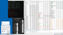
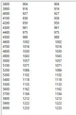
Neu BIOS fuer weisse Apex (2002) finde ich besser. Mein 8000C36-46-66 war nie in leben Y stable. Letzte Zeit konnte ich max 10 min laufen lassen. Immer VT3 Fehler.
Update gemacht, sofort 30 minute lang ging. TM5 ist immer stable, egal was fuer eine Spannungen. Immer VT3...
Ich denke, es liegt an CPU quality. OC Profil gehts gut ohne Problem 24/7.
Lange Zeit habe ich schon aufgehoert mit RAM OC, nur wegen neuem BIOS getestet habe. Halbe Stunde ist so was")
Mit dem Handy genau vor dem Fehler unter Last ein Bild gemacht. Knapp...
Naja, schwach CPU oder irgendwas. B Version, ich bin Noob
Man kann es nutzen in Alltags ohne Problem.
Update gemacht, sofort 30 minute lang ging. TM5 ist immer stable, egal was fuer eine Spannungen. Immer VT3...
Ich denke, es liegt an CPU quality. OC Profil gehts gut ohne Problem 24/7.
Lange Zeit habe ich schon aufgehoert mit RAM OC, nur wegen neuem BIOS getestet habe. Halbe Stunde ist so was
Mit dem Handy genau vor dem Fehler unter Last ein Bild gemacht. Knapp...
Naja, schwach CPU oder irgendwas. B Version, ich bin Noob
Man kann es nutzen in Alltags ohne Problem.
[2024/02/27 00:28:00]
Ai Overclock Tuner [Manual]
BCLK Frequency [100.0000]
PCIE Frequency [100.0000]
Intel(R) Adaptive Boost Technology [Auto]
ASUS MultiCore Enhancement [Enabled – Remove All limits (90°C)]
SVID Behavior [Trained]
BCLK Frequency : DRAM Frequency Ratio [100:100]
Memory Controller : DRAM Frequency Ratio [1:2]
DRAM Frequency [DDR5-8000MHz]
Performance Core Ratio [By Core Usage]
1-Core Ratio Limit [60]
2-Core Ratio Limit [59]
3-Core Ratio Limit [58]
4-Core Ratio Limit [57]
5-Core Ratio Limit [57]
6-Core Ratio Limit [56]
7-Core Ratio Limit [55]
8-Core Ratio Limit [55]
Performance Core0 Specific Ratio Limit [Auto]
Performance Core0 specific Voltage [Auto]
Performance Core1 Specific Ratio Limit [Auto]
Performance Core1 specific Voltage [Auto]
*Performance Core2 Specific Ratio Limit [Auto]
Performance Core2 specific Voltage [Auto]
*Performance Core3 Specific Ratio Limit [Auto]
Performance Core3 specific Voltage [Auto]
Performance Core4 Specific Ratio Limit [Auto]
Performance Core4 specific Voltage [Auto]
Performance Core5 Specific Ratio Limit [Auto]
Performance Core5 specific Voltage [Auto]
Performance Core6 Specific Ratio Limit [Auto]
Performance Core6 specific Voltage [Auto]
Performance Core7 Specific Ratio Limit [Auto]
Performance Core7 specific Voltage [Auto]
Efficient Core Ratio [By Core Usage]
Efficient Turbo Ratio Limit 1 [44]
Efficient Turbo Ratio Cores 1 [Auto]
Efficient Core Group0 Specific Ratio Limit [Auto]
Efficient Core Group0 specific Voltage [Auto]
Efficient Core Group1 Specific Ratio Limit [Auto]
Efficient Core Group1 specific Voltage [Auto]
Efficient Core Group2 Specific Ratio Limit [Auto]
Efficient Core Group2 specific Voltage [Auto]
Efficient Core Group3 Specific Ratio Limit [Auto]
Efficient Core Group3 specific Voltage [Auto]
AVX2 [Auto]
AVX2 Ratio Offset to per-core Ratio Limit [Auto]
AVX2 Voltage Guardband Scale Factor [Auto]
Maximus Tweak [Mode 2]
DRAM CAS# Latency [36]
DRAM RAS# to CAS# Delay Read [46]
DRAM RAS# to CAS# Delay Write [26]
DRAM RAS# PRE Time [46]
DRAM RAS# ACT Time [66]
DRAM Command Rate [2N]
DRAM RAS# to RAS# Delay L [12]
DRAM RAS# to RAS# Delay S [8]
DRAM REF Cycle Time 2 [544]
DRAM REF Cycle Time Same Bank [480]
DRAM Refresh Interval [131071]
DRAM WRITE Recovery Time [24]
DRAM READ to PRE Time [12]
DRAM FOUR ACT WIN Time [32]
DRAM WRITE to READ Delay L [24]
DRAM WRITE to READ Delay S [8]
DRAM CKE Minimum Pulse Width [20]
DRAM Write Latency [34]
Ctl0 dqvrefup [170]
Ctl0 dqvrefdn [88]
Ctl0 dqodtvrefup [Auto]
Ctl0 dqodtvrefdn [Auto]
Ctl1 cmdvrefup [Auto]
Ctl1 ctlvrefup [Auto]
Ctl1 clkvrefup [Auto]
Ctl1 ckecsvrefup [Auto]
Ctl2 cmdvrefdn [Auto]
Ctl2 ctlvrefdn [Auto]
Ctl2 clkvrefdn [Auto]
Read Equalization RxEq Start Sign [-]
Read Equalization RxEq Start [Auto]
Read Equalization RxEq Stop Sign [-]
Read Equalization RxEq Stop [Auto]
ODT_READ_DURATION [Auto]
ODT_READ_DELAY [Auto]
ODT_WRITE_DURATION [Auto]
ODT_WRITE_DELAY [Auto]
DQ RTT WR [40 DRAM Clock]
DQ RTT NOM RD [40 DRAM Clock]
DQ RTT NOM WR [34 DRAM Clock]
DQ RTT PARK [34 DRAM Clock]
DQ RTT PARK DQS [34 DRAM Clock]
GroupA CA ODT [240 DRAM Clock]
GroupA CS ODT [0 DRAM Clock]
GroupA CK ODT [0 DRAM Clock]
GroupB CA ODT [60 DRAM Clock]
GroupB CS ODT [40 DRAM Clock]
GroupB CK ODT [40 DRAM Clock]
Pull-up Output Driver Impedance [48 DRAM Clock]
Pull-Down Output Driver Impedance [40 DRAM Clock]
DQ RTT WR [40 DRAM Clock]
DQ RTT NOM RD [40 DRAM Clock]
DQ RTT NOM WR [34 DRAM Clock]
DQ RTT PARK [34 DRAM Clock]
DQ RTT PARK DQS [34 DRAM Clock]
GroupA CA ODT [240 DRAM Clock]
GroupA CS ODT [0 DRAM Clock]
GroupA CK ODT [0 DRAM Clock]
GroupB CA ODT [60 DRAM Clock]
GroupB CS ODT [40 DRAM Clock]
GroupB CK ODT [40 DRAM Clock]
Pull-up Output Driver Impedance [40 DRAM Clock]
Pull-Down Output Driver Impedance [48 DRAM Clock]
Round Trip Latency Init Value MC0 CHA [Auto]
Round Trip Latency Max Value MC0 CHA [Auto]
Round Trip Latency Offset Value Mode Sign MC0 CHA [-]
Round Trip Latency Offset Value MC0 CHA [Auto]
Round Trip Latency Init Value MC0 CHB [Auto]
Round Trip Latency Max Value MC0 CHB [Auto]
Round Trip Latency Offset Value Mode Sign MC0 CHB [-]
Round Trip Latency Offset Value MC0 CHB [Auto]
Round Trip Latency Init Value MC1 CHA [Auto]
Round Trip Latency Max Value MC1 CHA [Auto]
Round Trip Latency Offset Value Mode Sign MC1 CHA [-]
Round Trip Latency Offset Value MC1 CHA [Auto]
Round Trip Latency Init Value MC1 CHB [Auto]
Round Trip Latency Max Value MC1 CHB [Auto]
Round Trip Latency Offset Value Mode Sign MC1 CHB [-]
Round Trip Latency Offset Value MC1 CHB [Auto]
Round Trip Latency MC0 CHA R0 [Auto]
Round Trip Latency MC0 CHA R1 [Auto]
Round Trip Latency MC0 CHA R2 [0]
Round Trip Latency MC0 CHA R3 [0]
Round Trip Latency MC0 CHA R4 [0]
Round Trip Latency MC0 CHA R5 [0]
Round Trip Latency MC0 CHA R6 [0]
Round Trip Latency MC0 CHA R7 [0]
Round Trip Latency MC0 CHB R0 [Auto]
Round Trip Latency MC0 CHB R1 [Auto]
Round Trip Latency MC0 CHB R2 [0]
Round Trip Latency MC0 CHB R3 [0]
Round Trip Latency MC0 CHB R4 [0]
Round Trip Latency MC0 CHB R5 [0]
Round Trip Latency MC0 CHB R6 [0]
Round Trip Latency MC0 CHB R7 [0]
Round Trip Latency MC1 CHA R0 [Auto]
Round Trip Latency MC1 CHA R1 [Auto]
Round Trip Latency MC1 CHA R2 [0]
Round Trip Latency MC1 CHA R3 [0]
Round Trip Latency MC1 CHA R4 [0]
Round Trip Latency MC1 CHA R5 [0]
Round Trip Latency MC1 CHA R6 [0]
Round Trip Latency MC1 CHA R7 [0]
Round Trip Latency MC1 CHB R0 [Auto]
Round Trip Latency MC1 CHB R1 [Auto]
Round Trip Latency MC1 CHB R2 [0]
Round Trip Latency MC1 CHB R3 [0]
Round Trip Latency MC1 CHB R4 [0]
Round Trip Latency MC1 CHB R5 [0]
Round Trip Latency MC1 CHB R6 [0]
Round Trip Latency MC1 CHB R7 [0]
Early Command Training [Auto]
SenseAmp Offset Training [Auto]
Early ReadMPR Timing Centering 2D [Auto]
Read MPR Training [Auto]
Receive Enable Training [Auto]
Jedec Write Leveling [Auto]
Early Write Time Centering 2D [Auto]
Early Read Time Centering 2D [Auto]
Write Timing Centering 1D [Auto]
Write Voltage Centering 1D [Auto]
Read Timing Centering 1D [Auto]
Read Timing Centering with JR [Auto]
Dimm ODT Training* [Disabled]
Max RTT_WR [ODT Off]
DIMM RON Training* [Disabled]
Write Drive Strength/Equalization 2D* [Auto]
Write Slew Rate Training* [Auto]
Read ODT Training* [Disabled]
Comp Optimization Training [Auto]
Read Equalization Training* [Auto]
Read Amplifier Training* [Auto]
Write Timing Centering 2D [Auto]
Read Timing Centering 2D [Auto]
Command Voltage Centering [Auto]
Early Command Voltage Centering [Auto]
Write Voltage Centering 2D [Auto]
Read Voltage Centering 2D [Auto]
Late Command Training [Auto]
Round Trip Latency [Auto]
Turn Around Timing Training [Auto]
CMD CTL CLK Slew Rate [Auto]
CMD/CTL DS & E 2D [Auto]
Read Voltage Centering 1D [Auto]
TxDqTCO Comp Training* [Auto]
ClkTCO Comp Training* [Auto]
TxDqsTCO Comp Training* [Auto]
VccDLL Bypass Training [Auto]
CMD/CTL Drive Strength Up/Dn 2D [Auto]
DIMM CA ODT Training [Auto]
PanicVttDnLp Training* [Auto]
Read Vref Decap Training* [Auto]
Vddq Training [Disabled]
Duty Cycle Correction Training [Auto]
Periodic DCC [Auto]
Rank Margin Tool Per Bit [Auto]
DIMM DFE Training [Auto]
EARLY DIMM DFE Training [Auto]
Tx Dqs Dcc Training [Auto]
DRAM DCA Training [Auto]
Write Driver Strength Training [Auto]
Rank Margin Tool [Auto]
Memory Test [Auto]
DIMM SPD Alias Test [Auto]
Receive Enable Centering 1D [Auto]
Retrain Margin Check [Auto]
Write Drive Strength Up/Dn independently [Auto]
LPDDR DqDqs Re-Training [Auto]
Margin Check Limit [Disabled]
tRDRD_sg_Training [Auto]
tRDRD_sg_Runtime [16]
tRDRD_dg_Training [Auto]
tRDRD_dg_Runtime [8]
tRDWR_sg [20]
tRDWR_dg [20]
tWRWR_sg [16]
tWRWR_dg [8]
tWRRD_sg [Auto]
tWRRD_dg [Auto]
tRDRD_dr [0]
tRDRD_dd [0]
tRDWR_dr [0]
tRDWR_dd [0]
tWRWR_dr [0]
tWRWR_dd [0]
tWRRD_dr [0]
tWRRD_dd [0]
tRPRE [Auto]
tWPRE [Auto]
tWPOST [Auto]
tWRPRE [Auto]
tPRPDEN [Auto]
tRDPDEN [Auto]
tWRPDEN [Auto]
tCPDED [20]
tREFIX9 [Auto]
Ref Interval [Auto]
tXPDLL [Auto]
tXP [30]
tPPD [2]
tCCD_L_tDLLK [Auto]
tZQCAL [Auto]
tZQCS [Auto]
OREF_RI [Auto]
Refresh Watermarks [High]
Refresh Hp Wm [Auto]
Refresh Panic Wm [Auto]
Refresh Abr Release [Auto]
tXSDLL [Auto]
tZQOPER [Auto]
tMOD [Auto]
CounttREFIWhileRefEn [Auto]
HPRefOnMRS [Auto]
SRX Ref Debits [Auto]
RAISE BLK WAIT [Auto]
Ref Stagger En [Auto]
Ref Stagger Mode [Auto]
Disable Stolen Refresh [Auto]
En Ref Type Display [Auto]
Trefipulse Stagger Disable [Auto]
tRPab ext [Auto]
derating ext [Auto]
Allow 2cyc B2B LPDDR [Auto]
tCSH [Auto]
tCSL [Auto]
powerdown Enable [Auto]
idle length [Auto]
raise cke after exit latency [Auto]
powerdown latency [Auto]
powerdown length [Auto]
selfrefresh latency [Auto]
selfrefresh length [Auto]
ckevalid length [Auto]
ckevalid enable [Auto]
idle enable [Auto]
selfrefresh enable [Auto]
Address mirror [Auto]
no gear4 param divide [Auto]
x8 device [Auto]
no gear2 param divide [Auto]
ddr 1dpc split ranks on subch [Auto]
write0 enable [Auto]
MultiCycCmd [Auto]
WCKDiffLowInIdle [Auto]
PBR Disable [Auto]
PBR OOO Dis [Auto]
PBR Disable on hot [Auto]
PBR Exit on Idle Cnt [Auto]
tXSR [Auto]
Dec tCWL [Auto]
Add tCWL [Auto]
Add 1Qclk delay [Auto]
MRC Fast Boot [Disabled]
MCH Full Check [Auto]
Mem Over Clock Fail Count [3]
Training Profile [Auto]
RxDfe [Auto]
Mrc Training Loop Count [3]
DRAM CLK Period [Auto]
Dll_bwsel [Auto]
Controller 0, Channel 0 Control [Enabled]
Controller 0, Channel 1 Control [Enabled]
Controller 1, Channel 0 Control [Enabled]
Controller 1, Channel 1 Control [Enabled]
MC_Vref0 [Auto]
MC_Vref1 [Auto]
MC_Vref2 [Auto]
Fine Granularity Refresh mode [Auto]
SDRAM Density Per Die [Auto]
SDRAM Banks Per Bank Group [Auto]
SDRAM Bank Groups [Auto]
Dynamic Memory Boost [Disabled]
Realtime Memory Frequency [Disabled]
SA GV [Disabled]
Voltage Monitor [Die Sense]
VRM Initialization Check [Enabled]
CPU Input Voltage Load-line Calibration [Auto]
CPU Load-line Calibration [Level 4:Recommended for OC]
Synch ACDC Loadline with VRM Loadline [Disabled]
CPU Current Capability [140%]
CPU Current Reporting [Auto]
Core Voltage Suspension [Auto]
CPU VRM Switching Frequency [Auto]
VRM Spread Spectrum [Auto]
CPU Power Duty Control [Auto]
CPU Power Phase Control [Auto]
CPU Power Thermal Control [125]
CPU Core/Cache Boot Voltage [Auto]
CPU Input Boot Voltage [Auto]
PLL Termination Boot Voltage [Auto]
CPU Standby Boot Voltage [Auto]
Memory Controller Boot Voltage [Auto]
CPU Core Auto Voltage Cap [Auto]
CPU Input Auto Voltage Cap [Auto]
Memory Controller Auto Voltage Cap [Auto]
Fast Throttle Threshold [Auto]
Package Temperature Threshold [Auto]
Regulate Frequency by above Threshold [Auto]
IVR Transmitter VDDQ ICCMAX [Auto]
Unlimited ICCMAX [Auto]
CPU Core/Cache Current Limit Max. [400.00]
Long Duration Package Power Limit [320]
Package Power Time Window [Auto]
Short Duration Package Power Limit [330]
Dual Tau Boost [Disabled]
IA AC Load Line [0.32]
IA DC Load Line [Auto]
IA CEP [Disabled]
SA CEP [Disabled]
IA SoC Iccmax Reactive Protector [Disabled]
Inverse Temperature Dependency Throttle [Auto]
IA VR Voltage Limit [1580]
CPU SVID Support [Auto]
Cache Dynamic OC Switcher [Disabled]
TVB Voltage Optimizations [Disabled]
Enhanced TVB [Disabled]
Overclocking TVB [Disabled]
Overclocking TVB Global Temperature Offset Sign [+]
Overclocking TVB Global Temperature Offset Value [Auto]
Offset Mode Sign 1 [-]
V/F Point 1 Offset [0.01800]
Offset Mode Sign 2 [-]
V/F Point 2 Offset [0.00800]
Offset Mode Sign 3 [+]
V/F Point 3 Offset [0.03000]
Offset Mode Sign 4 [+]
V/F Point 4 Offset [0.04000]
Offset Mode Sign 5 [+]
V/F Point 5 Offset [0.03000]
Offset Mode Sign 6 [-]
V/F Point 6 Offset [0.03000]
Offset Mode Sign 7 [-]
V/F Point 7 Offset [0.10400]
Offset Mode Sign 8 [-]
V/F Point 8 Offset [0.10400]
Offset Mode Sign 9 [-]
V/F Point 9 Offset [0.15600]
Offset Mode Sign 10 [-]
V/F Point 10 Offset [0.15600]
Offset Mode Sign 11 [-]
V/F Point 11 Offset [0.15100]
Initial BCLK Frequency [Auto]
Runtime BCLK OC [Auto]
BCLK Amplitude [Auto]
BCLK Slew Rate [Auto]
BCLK Spread Spectrum [Auto]
Initial PCIE Frequency [Auto]
PCIE/DMI Amplitude [Auto]
PCIE/DMI Slew Rate [Auto]
PCIE/DMI Spread Spectrum [Auto]
Cold Boot PCIE Frequency [Auto]
Realtime Memory Timing [Disabled]
SPD Write Disable [TRUE]
PVD Ratio Threshold [Auto]
SA PLL Frequency Override [Auto]
BCLK TSC HW Fixup [Enabled]
Core Ratio Extension Mode [Disabled]
FLL OC mode [Auto]
UnderVolt Protection [Disabled]
Switch Microcode [Current Microcode]
Xtreme Tweaking [Disabled]
Core PLL Voltage [Auto]
GT PLL Voltage [Auto]
Ring PLL Voltage [Auto]
System Agent PLL Voltage [Auto]
Memory Controller PLL Voltage [Auto]
Efficient-core PLL Voltage [Auto]
CPU 1.8V Small Rail [Auto]
PLL Termination Voltage [Auto]
CPU Standby Voltage [Auto]
PCH 1.05V Voltage [Auto]
PCH 0.82V Voltage [Auto]
CPU Input Voltage Reset Voltage [Auto]
Eventual CPU Input Voltage [Auto]
Eventual Memory Controller Voltage [Auto]
Package Temperature Threshold [Auto]
Regulate Frequency by above Threshold [Auto]
Cooler Efficiency Customize [Keep Training]
Cooler Re-evaluation Algorithm [Normal]
Optimism Scale [100]
Ring Down Bin [Auto]
Min. CPU Cache Ratio [Auto]
Max. CPU Cache Ratio [49]
BCLK Aware Adaptive Voltage [Auto]
Actual VRM Core Voltage [Auto]
Global Core SVID Voltage [Auto]
Cache SVID Voltage [Auto]
CPU L2 Voltage [Auto]
CPU System Agent Voltage [Manual Mode]
- CPU System Agent Voltage Override [1.14000]
CPU Input Voltage [Auto]
High DRAM Voltage Mode [Enabled]
DRAM VDD Voltage [1.50000]
DRAM VDDQ Voltage [1.47000]
IVR Transmitter VDDQ Voltage [1.26500]
Memory Controller Voltage [1.36250]
MC Voltage Calculation Voltage Base [Auto]
VDD Calculation Voltage Base [Auto]
PMIC Voltages [Sync All PMICs]
SPD HUB VLDO (1.8V) [1.80000]
SPD HUB VDDIO (1.0V) [1.00000]
DRAM VDD Voltage [1.50000]
DRAM VDDQ Voltage [1.47000]
DRAM VPP Voltage [1.81500]
DRAM VDD Switching Frequency [1.50000]
DRAM VDDQ Switching Frequency [1.50000]
DRAM VPP Switching Frequency [1.50000]
DRAM Current Capability [7.87500]
PCI Express Native Power Management [Enabled]
Native ASPM [Disabled]
DMI Link ASPM Control [Disabled]
ASPM [Auto]
L1 Substates [Disabled]
DMI ASPM [Disabled]
DMI Gen3 ASPM [Disabled]
PEG - ASPM [Disabled]
PCI Express Clock Gating [Enabled]
Hardware Prefetcher [Enabled]
Adjacent Cache Line Prefetch [Enabled]
Intel (VMX) Virtualization Technology [Disabled]
Per P-Core Control [Disabled]
Per E-Core Control [Disabled]
Active Performance Cores [All]
Active Efficient Cores [All]
Hyper-Threading [Enabled]
Hyper-Threading of Core 0 [Enabled]
Hyper-Threading of Core 1 [Enabled]
Hyper-Threading of Core 2 [Enabled]
Hyper-Threading of Core 3 [Enabled]
Hyper-Threading of Core 4 [Enabled]
Hyper-Threading of Core 5 [Enabled]
Hyper-Threading of Core 6 [Enabled]
Hyper-Threading of Core 7 [Enabled]
Total Memory Encryption [Disabled]
Legacy Game Compatibility Mode [Disabled]
Boot performance mode [Auto]
Intel(R) SpeedStep(tm) [Enabled]
Intel(R) Speed Shift Technology [Enabled]
Intel(R) Turbo Boost Max Technology 3.0 [Enabled]
Turbo Mode [Enabled]
Acoustic Noise Mitigation [Disabled]
CPU C-states [Auto]
Thermal Monitor [Enabled]
Dual Tau Boost [Disabled]
VT-d [Disabled]
Memory Remap [Enabled]
Enable VMD controller [Enabled]
Map PCIE Storage under VMD [Disabled]
Map SATA Controller under VMD [Disabled]
M.2_1 Link Speed [Auto]
PCIEX16(G5)_1 Link Speed [Auto]
PCIEX16(G5)_2 Link Speed [Auto]
PCIEX1(G4) Link Speed [Auto]
PCIEX4(G4) Link Speed [Auto]
M.2_2 Link Speed [Auto]
DIMM.2_1 Link Speed [Auto]
DIMM.2_2 Link Speed [Auto]
SATA Controller(s) [Enabled]
Aggressive LPM Support [Disabled]
SMART Self Test [Enabled]
M.2_3 [Enabled]
M.2_3 Hot Plug [Disabled]
SATA6G_1 [Enabled]
SATA6G_1 Hot Plug [Disabled]
SATA6G_2 [Enabled]
SATA6G_2 Hot Plug [Disabled]
SATA6G_3 [Enabled]
SATA6G_3 Hot Plug [Disabled]
SATA6G_4 [Enabled]
SATA6G_4 Hot Plug [Disabled]
PTT [Enable]
Intel(R) Dynamic Tuning Technology [Disabled]
PCIE Tunneling over USB4 [Enabled]
Discrete Thunderbolt(TM) Support [Disabled]
Security Device Support [Enable]
SHA256 PCR Bank [Enabled]
Pending operation [None]
Platform Hierarchy [Enabled]
Storage Hierarchy [Enabled]
Endorsement Hierarchy [Enabled]
Physical Presence Spec Version [1.3]
Disable Block Sid [Disabled]
USB Host Controller Support [Disabled]
Password protection of Runtime Variables [Enable]
Above 4G Decoding [Enabled]
Resize BAR Support [Enabled]
SR-IOV Support [Disabled]
Legacy USB Support [Enabled]
XHCI Hand-off [Enabled]
SanDisk [Auto]
LAN_U32G2_1 [Enabled]
U32G1_E5 [Enabled]
U32G1_E6 [Enabled]
U32G1_E7 [Enabled]
U32G1_E8 [Enabled]
U32G2X2_C3 [Enabled]
U32G2_5 [Enabled]
U32G2_6 [Enabled]
U32G2_7 [Enabled]
U32G2_P8 [Enabled]
U32G2X2_C9 [Enabled]
U32G1_E1 [Enabled]
U32G1_E2 [Enabled]
U32G1_E3 [Enabled]
U32G1_E4 [Enabled]
Network Stack [Disabled]
Device [N/A]
Restore AC Power Loss [Power Off]
Max Power Saving [Disabled]
ErP Ready [Disabled]
Power On By PCI-E [Disabled]
Power On By RTC [Disabled]
USB Audio [Enabled]
Intel LAN [Enabled]
USB power delivery in Soft Off state (S5) [Disabled]
Connectivity mode (Wi-Fi & Bluetooth) [Enabled]
When system is in working state [All On]
Q-Code LED Function [Auto]
When system is in sleep, hibernate or soft off states [All On]
M.2_2 Configuration [Auto]
ASMedia USB 3.2 Controller_U32G1_E12 [Enabled]
ASMedia USB 3.2 Controller_U32G1_E34 [Enabled]
GNA Device [Disabled]
ASMedia Storage Controller [Enabled]
Windows Hot-plug Notification [Disabled]
ASPM Support [Disabled]
CPU Temperature [Monitor]
CPU Package Temperature [Monitor]
MotherBoard Temperature [Monitor]
VRM Temperature [Monitor]
Chipset Temperature [Monitor]
T_Sensor Temperature [Monitor]
DIMM.2 Sensor 1 Temperature [Monitor]
DIMM.2 Sensor 2 Temperature [Monitor]
Water In T Sensor Temperature [Monitor]
Water Out T Sensor Temperature [Monitor]
DIMM A1 Temperature [Monitor]
DIMM B1 Temperature [Monitor]
CPU Fan Speed [Monitor]
CPU Optional Fan Speed [Monitor]
Chassis Fan 1 Speed [Monitor]
Chassis Fan 2 Speed [Monitor]
Chassis Fan 3 Speed [Monitor]
Water Pump+ Speed [Monitor]
AIO Pump Speed [Monitor]
Flow Rate [Monitor]
CPU Core Voltage [Monitor]
12V Voltage [Monitor]
5V Voltage [Monitor]
3.3V Voltage [Monitor]
Memory Controller Voltage [Monitor]
CPU Fan Q-Fan Control [DC Mode]
CPU Fan Profile [Standard]
CPU Fan Q-Fan Source [CPU]
CPU Fan Step Up [Level 0]
CPU Fan Step Down [Level 4]
CPU Fan Speed Low Limit [200 RPM]
Chassis Fan 1 Q-Fan Control [Auto Detect]
Chassis Fan 1 Profile [Standard]
Chassis Fan 1 Q-Fan Source [CPU]
Chassis Fan 1 Step Up [Level 0]
Chassis Fan 1 Step Down [Level 0]
Chassis Fan 1 Speed Low Limit [200 RPM]
Chassis Fan 2 Q-Fan Control [PWM Mode]
Chassis Fan 2 Profile [Standard]
Chassis Fan 2 Q-Fan Source [Chipset]
Chassis Fan 2 Step Up [Level 0]
Chassis Fan 2 Step Down [Level 4]
Chassis Fan 2 Speed Low Limit [200 RPM]
Chassis Fan 3 Q-Fan Control [DC Mode]
Chassis Fan 3 Profile [Silent]
Chassis Fan 3 Q-Fan Source [CPU]
Chassis Fan 3 Step Up [Level 0]
Chassis Fan 3 Step Down [Level 0]
Chassis Fan 3 Speed Low Limit [200 RPM]
Water Pump+ Q-Fan Control [PWM Mode]
Water Pump+ Profile [Manual]
Water Pump+ Q-Fan Source [CPU]
Water Pump+ Step Up [Level 0]
Water Pump+ Step Down [Level 4]
Water Pump+ Speed Low Limit [Ignore]
Water Pump+ Point4 Temperature [70]
Water Pump+ Point4 Duty Cycle (%) [100]
Water Pump+ Point3 Temperature [50]
Water Pump+ Point3 Duty Cycle (%) [85]
Water Pump+ Point2 Temperature [40]
Water Pump+ Point2 Duty Cycle (%) [80]
Water Pump+ Point1 Temperature [25]
Water Pump+ Point1 Duty Cycle (%) [60]
AIO Pump Q-Fan Control [Auto Detect]
AIO Pump Profile [Full Speed]
CPU Temperature LED Switch [Enabled]
Launch CSM [Disabled]
OS Type [Other OS]
Secure Boot Mode [Custom]
Fast Boot [Enabled]
Next Boot after AC Power Loss [Fast Boot]
Boot Logo Display [Auto]
POST Delay Time [3 sec]
Bootup NumLock State [On]
Wait For 'F1' If Error [Enabled]
Option ROM Messages [Force BIOS]
Interrupt 19 Capture [Disabled]
AMI Native NVMe Driver Support [Enabled]
Setup Mode [Advanced Mode]
Boot Sector (MBR/GPT) Recovery Policy [Local User Control]
Next Boot Recovery Action [Skip]
BIOS Image Rollback Support [Enabled]
Publish HII Resources [Disabled]
Flexkey [Safe Boot]
Setup Animator [Disabled]
Load from Profile [1]
Profile Name [8000]
Save to Profile [1]
DIMM Slot Number [DIMM_A1]
Download & Install ARMOURY CRATE app [Disabled]
Download & Install MyASUS service & app [Disabled]
Anhänge
Zuletzt bearbeitet:
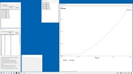
 Und es spuckt eine Zeit aus, die einem verrät, ob das neue Setting auch flotter ist. Dann kann man sich an längere Tests machen, wenn man das will.


")