


[Sammelthread] ASUS ROG Maximus XI Gene (90MB10E0-M0EAY0)
--- Produktseite | PDF-Handbuch | Support-Downloads | Preisvergleich | HWBOT ---
The Gene is back with the Maximus XI family, this time with a twist. Multi-GPU configurations are becoming rarer as NVIDIA and AMD focus on single-card performance, and GPU coolers are growing beyond two slots to improve performance and reduce noise. The old Gene’s dual-GPU focus doesn’t reflect the kinds of systems gamers and enthusiasts are building, so the new model refocuses to aggressively pursue higher performance and support additional storage. It has already made its mark on the hardware leaderboards by claiming 11 global first place scores and eight world records, including the fastest CPU frequency at 7613.19MHz and the highest memory clock at 5566MHz.
Spezifikationen
| CPU | Build in Intel® 9th / 8th Gen Intel® Core™, Pentium® Gold and Celeron® Processors Supports Intel® Turbo Boost Technology 2.0 * Refer to ASUS Deutschland for CPU support list |
| Chipset | Build in Intel® Z390 |
| Memory | Socket 1151 for 9th / 8th Gen Intel® Core™, Pentium® Gold and Celeron® processors 2 x DIMM, Max. 64GB, DDR4 4700(O.C)/4600(O.C)/4500(O.C)/4400(O.C)/4266(O.C.)/4133(O.C.)/4000(O.C.)/3866(O.C.)/3600(O.C.)/3466(O.C.)/3400(O.C.)/3333(O.C.)/3300(O.C.)/3200(O.C.)/3000(O.C.)/2933(O.C.)/2800(O.C.)/2666/2400(O.C.)/2133(O.C.) MHz Non-ECC, Un-buffered Memory * Dual Channel Memory Architecture Supports Intel® Extreme Memory Profile (XMP) * Refer to ASUS Deutschland for the Memory QVL (Qualified Vendors Lists). * Double Capcity DRAM support depends oh the DRAM models |
| Graphic | Integrated Graphics Processor- Intel® UHD Graphics support - Supports HDMI 1.4b with max. resolution 4096 x 2160 @ 30 Hz |
| Expansion Slots | Socket 1151 for 9th / 8th Gen Intel® Core™, Pentium® Gold and Celeron® processors 1 x PCIe 3.0 x16 Intel® Z390 Chipset 1 x PCIe 3.0 x4 |
| Storage | Socket 1151 for 9th / 8th Gen Intel® Core™, Pentium® Gold and Celeron® processors : 2 x ROG DIMM.2 Module support(CPU_DIMM.2), with M key, type 2242/2260/2280/22110 storage devices support (PCIE 3.0 x 4 mode) Intel® Z390 Chipset : 2 x M.2 Socket 3, with M Key, type 2242/2260/2280 storage devices support (x4 PCIE mode) Intel® Z390 Chipset : 4 x SATA 6Gb/s port(s), Support Raid 0, 1, 5, 10 Intel® Optane™ Memory Ready |
| LAN | Intel® I219V, 1 x Gigabit LAN Controller(s) Anti-surge LANGuard ROG GameFirst Technology |
| Wireless Data Network | Intel® Wireless-AC 9560 Wi-Fi 802.11 a/b/g/n/ac Supports dual band frequency 2.4/5 GHz Supports MU-MIMO Supports channel bandwidth: HT20/HT40/HT80/HT160. Up to 1.73Gbps transfer speed |
| Bluetooth | Bluetooth® 5.0 |
| Audio | ROG SupremeFX 8-Channel High Definition Audio CODEC S1220A - Impedance sense for front and rear headphone outputs - Supports : Jack-detection, Multi-streaming, Front Panel Jack-retasking - High quality 120 dB SNR stereo playback output 113 dB SNR recording input Audio Feature : - SupremeFX Shielding™ Technology - Gold-plated jacks - Optical S/PDIF out port(s) at back panel - Sonic Radar III - Sonic Studio III + Sonic Studio Link |
| USB Ports | Intel® Z390 Chipset : 1 x USB 3.1 Gen 2 front panel connector port(s) Intel® Z390 Chipset : 4 x USB 3.1 Gen 2 port(s) (3 x Type-A+1 x Type-C) Intel® Z390 Chipset : 8 x USB 3.1 Gen 1 port(s) (2 at mid-board) Intel® Z390 Chipset : 6 x USB 2.0 port(s) |
| ROG Exclusive Features | ROG CPU-Z ROG CloneDrive Pre-mounted I/O Shield Slow Mode CMOS button Overwolf ReTry Button Safe Boot Button Start Button Reset Button LN2 Mode ROG Aura - Aura Lighting Control - Aura RGB Strip Headers Extreme Engine Digi+ : - MicroFine Alloy Chokes - 10K Black Metallic Capacitors Mem TweakIt Double Power : - Dual 8 -pin CPU USB BIOS Flashback ROG Exclusive Software - RAMCache III - GameFirst V - Sonic Studio III + Sonic Studio Link - Sonic Radar III |
| Special Features | AI Overclocking ASUS 5X Protection III : - ASUS SafeSlot Core: Fortified PCIe Slot prevents damage - ASUS LANGuard: Protects against LAN surges, lightning strikes and static-electricity discharges! Gamer's Guardian: - SafeSlot ASUS Optimem II: - Optimem (Improved DDR4 stability) - Improved DDR4 Stability ASUS Exclusive Features : - MemOK! II - Pre-mounted I/O Shield - ASUS NODE : hardware control interface - BIOS Flashback Button - Clear CMOS Button - Reset Button ASUS Quiet Thermal Solution : - ASUS Fan Xpert 4 ASUS Q-Design : - ASUS Q-Code - ASUS Q-LED (CPU, VGA, Boot Device LED) - ASUS Q-Slot - ASUS Q-DIMM - ASUS Q-Connector AURA: RGB Lighting Control Armoury Crate |
| Operating System Support | Windows® 10 64-bit |
| Back I/O Ports | 1 x PS/2 keyboard/mouse combo port(s) 1 x HDMI 1 x LAN (RJ45) port(s) 3 x USB 3.1 Gen 2 (red)Type-A, 1 x USB 3.1 Gen 2 (red)Type-C 6 x USB 3.1 Gen 1 (blue) 2 x USB 2.0 1 x Clear CMOS button(s) 1 x Wi-Fi antenna port(s) |
| BIOS | 1 x 128 Mb Flash ROM, UEFI AMI BIOS, PnP, DMI3.0, WfM2.0, SM BIOS 3.0, ACPI 6.0, Multi-language BIOS, ASUS EZ Flash 3, CrashFree BIOS 3, F11 EZ Tuning Wizard, F6 Qfan Control, F3 My Favorites, Last Modified log, F12 PrintScreen, F3 Shortcut functions and ASUS DRAM SPD (Serial Presence Detect) memory information. |
| Manageability | WfM2.0, DMI3.0, WOL by PME, PXE |
| Support Disc | Overwolf 1-year Anti-Virus software Daemon Tools Software WinRAR |
| Form Factor | mATX Form Factor 9.6 inch x 8.9 inch ( 24.4 cm x 22.6 cm ) |
Backpanel:
Special Features
1) Double-capacity DIMM support (DC DIMM)
Maximus XI Gene features a unique memory-trace design that supports up to 32GB per slot for a total memory capacity of 64GB. With double-capacity UDIMM modules, Maximus XI Gene delivers four-DIMM memory capacity in a compact, dual-DIMM design.
--> [Sammelthread] Double Capacity DIMM DDR4 (DC DIMM)
2) Overclocker's toolkit
1) MEMOK! II - DRAM Auto Training Switch
2) QLED - 4 LEDs to show current boot status.
3) LN2 Mode - Jumper to enable special options and functions for liquid-nitrogen (LN2) overclocking.
4) Pause Switch - Activate to pause the system and fine-tune OC parameters mid-benchmark.
5) Slow Mode Switch - Instantly reduces the CPU ratio to 8X to bypass finicky benchmark passages.
6) ReTry Button - One press instantly initiates a hard reset.
7) Safe Boot Button - Instantly reset the PC and boot directly in to a safe mode.
8) ProbeIt - Check the voltage via integrated measurement points.
BIOS
Reguläre Releases (Support Downloads - BIOS Shortcut)
- 1502 (2020/04/29, Improved system stability)
- 1401 (2019/12/11, Improve Memory-OC rules & Intel Optane H10 compatibility, fixed Tjmax for i9-9900KS)
- 1302 (2019/09/11, Improve system stability)
- 1105 (2019/06/20, Improved DRAM compatibility & system performance & storage device comp, Updated ME to v12.0.39 & microcode for Security)
- 1005 (2019/04/25, Enhanced security. Improved SSD & DRAM compatibility, Updated RAID driver)
- 0905 (2019/04/11, Enhanced Security)
- 0903 (2019/03/22, Microcode Update)
- 0805 (2019/01/02, Supported JEDEC Standard DDR4 32GB memory, Updated RST driver & ME FW, Improve system performance & DRAM stability)
- 0702 (2018/12/18, Improved system stability and performance, updated RST Driver)
- 0602 (2018/10/31, Updated Microcode, improved DRAM stability, fixed USB issue)
- 0506 (2018/09/29, First Release BIOS)
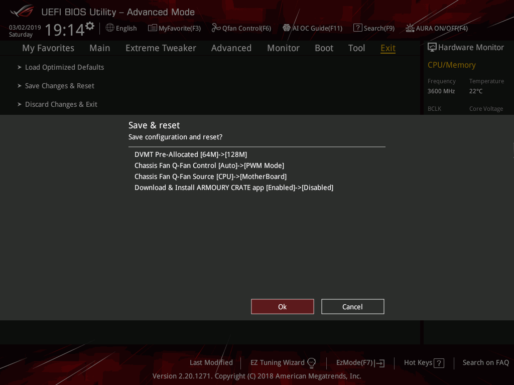
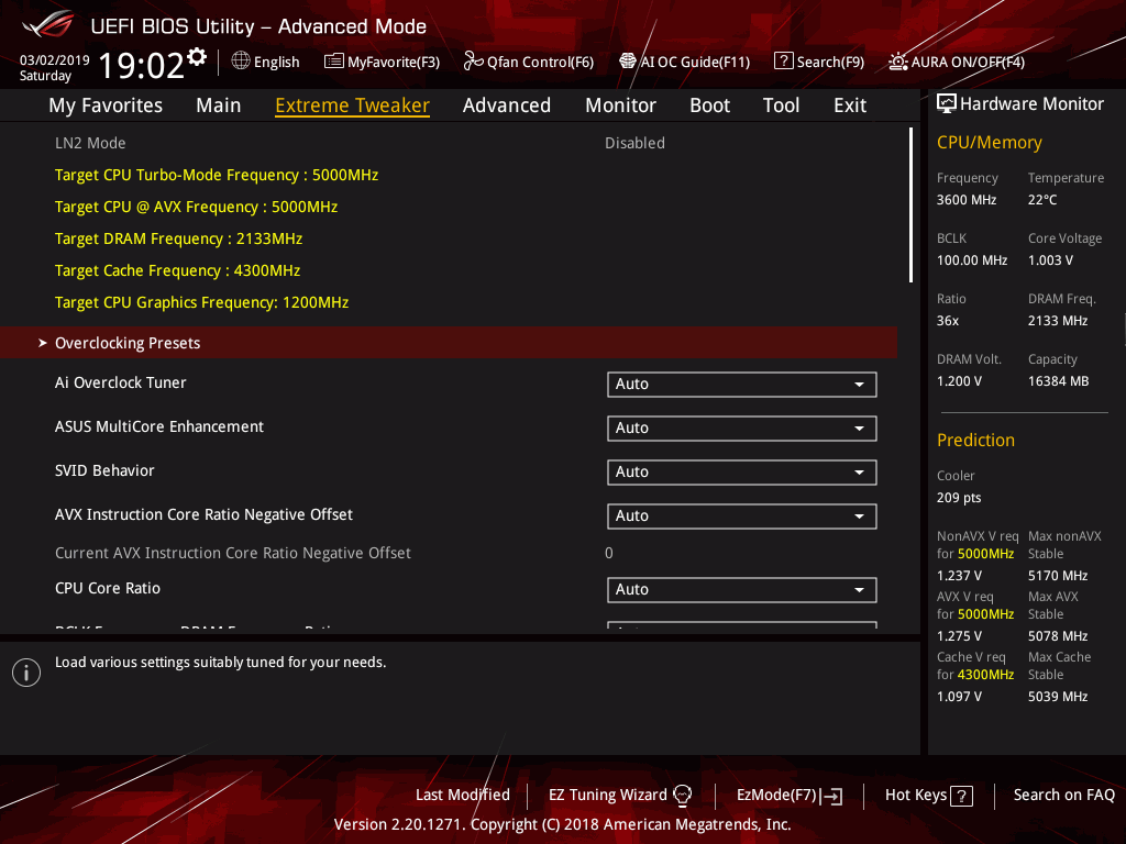
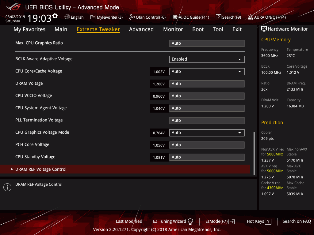
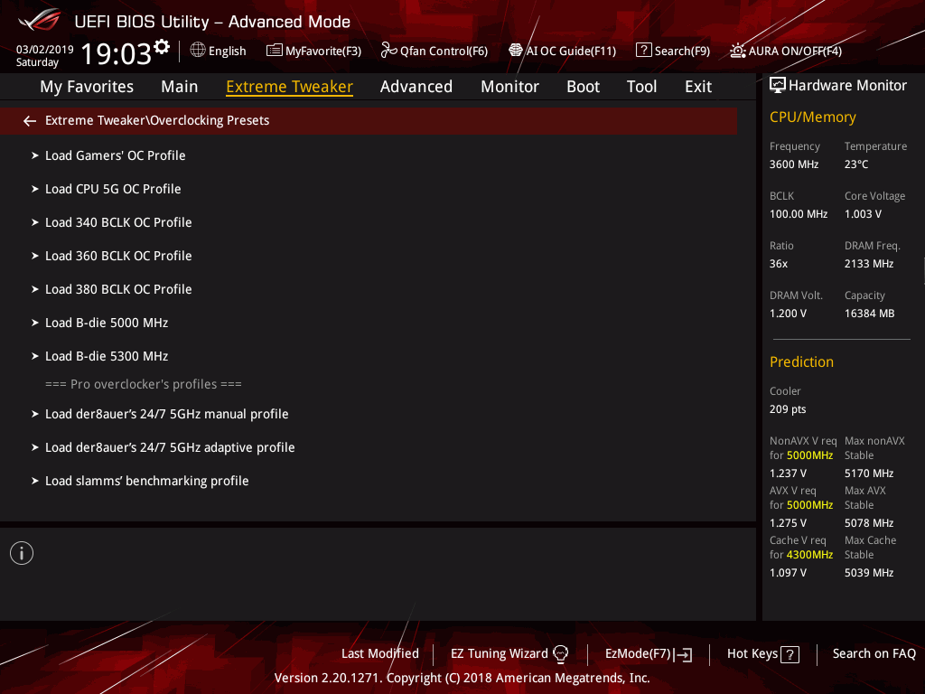
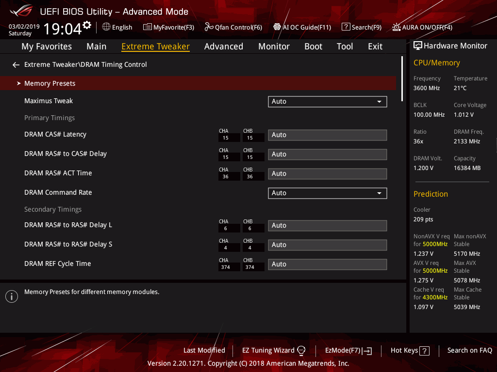
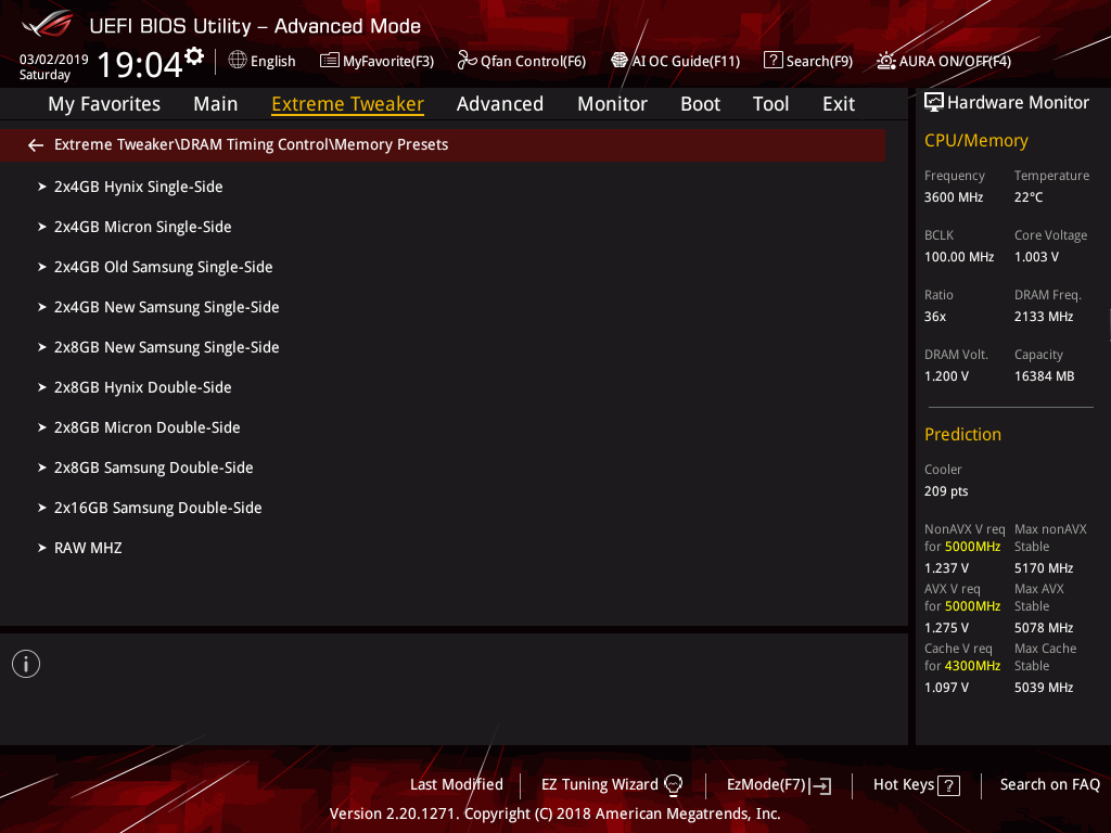
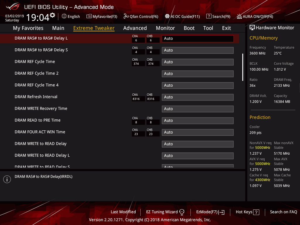
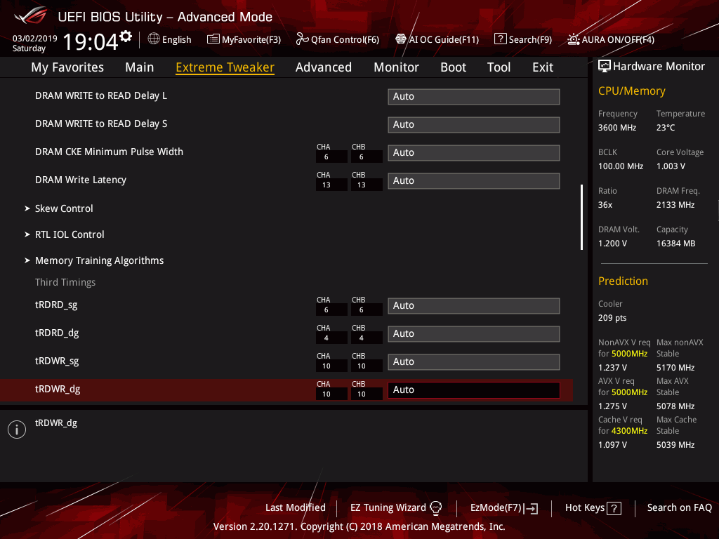
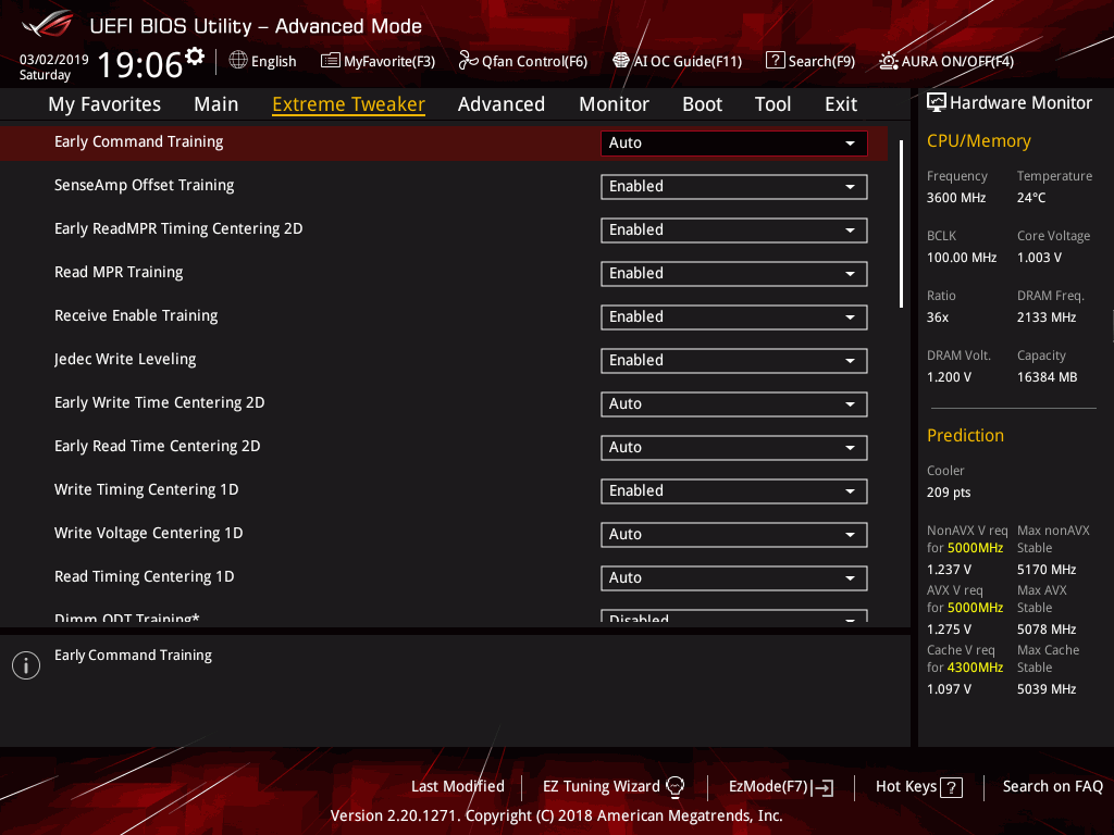
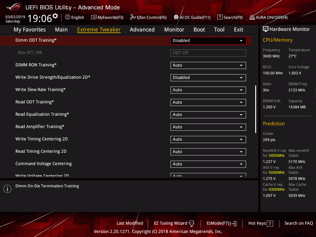
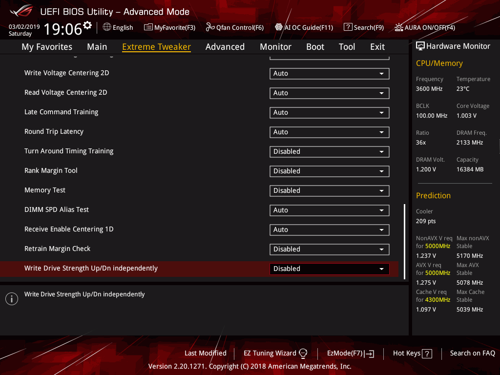
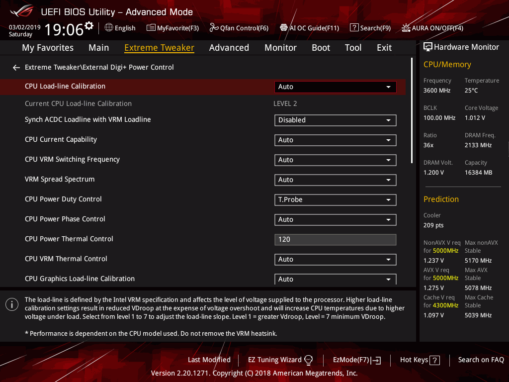
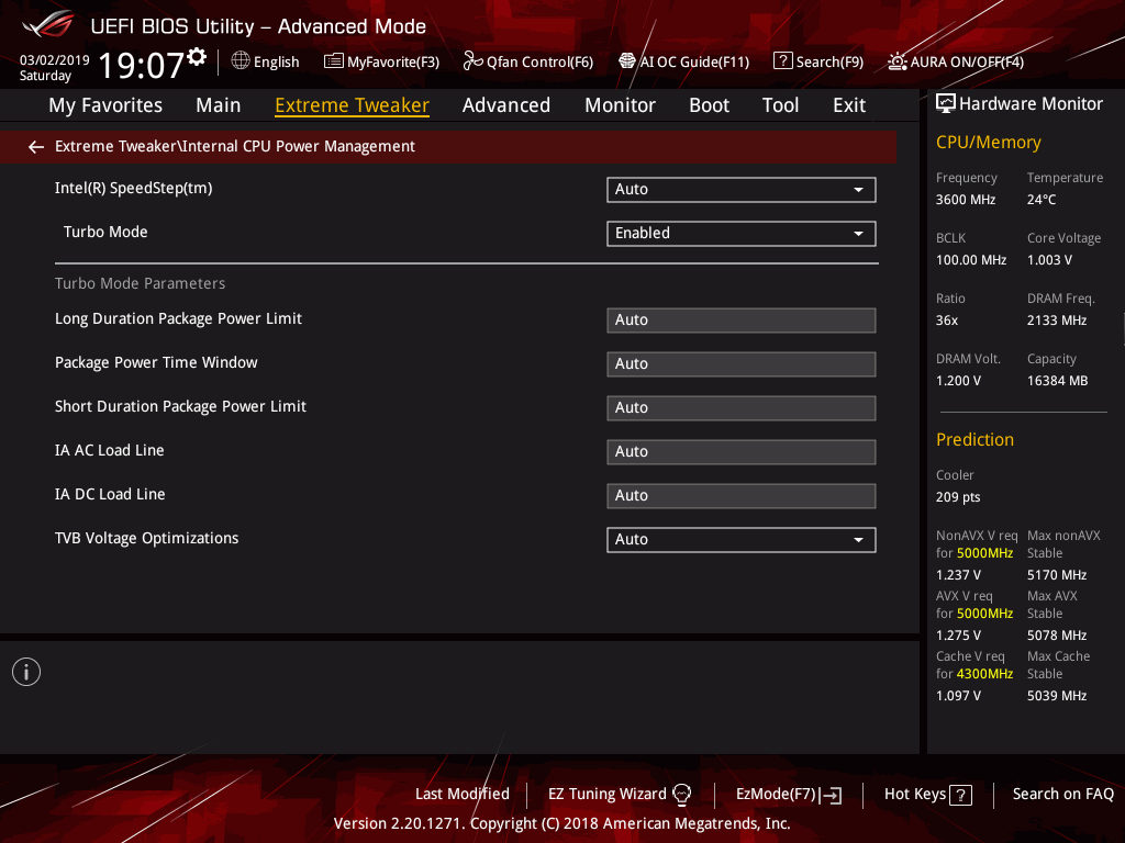
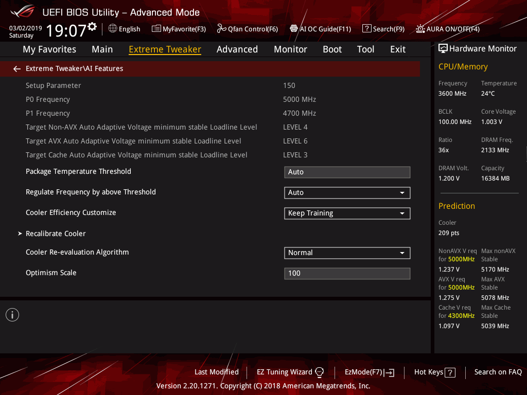
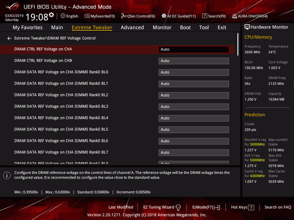
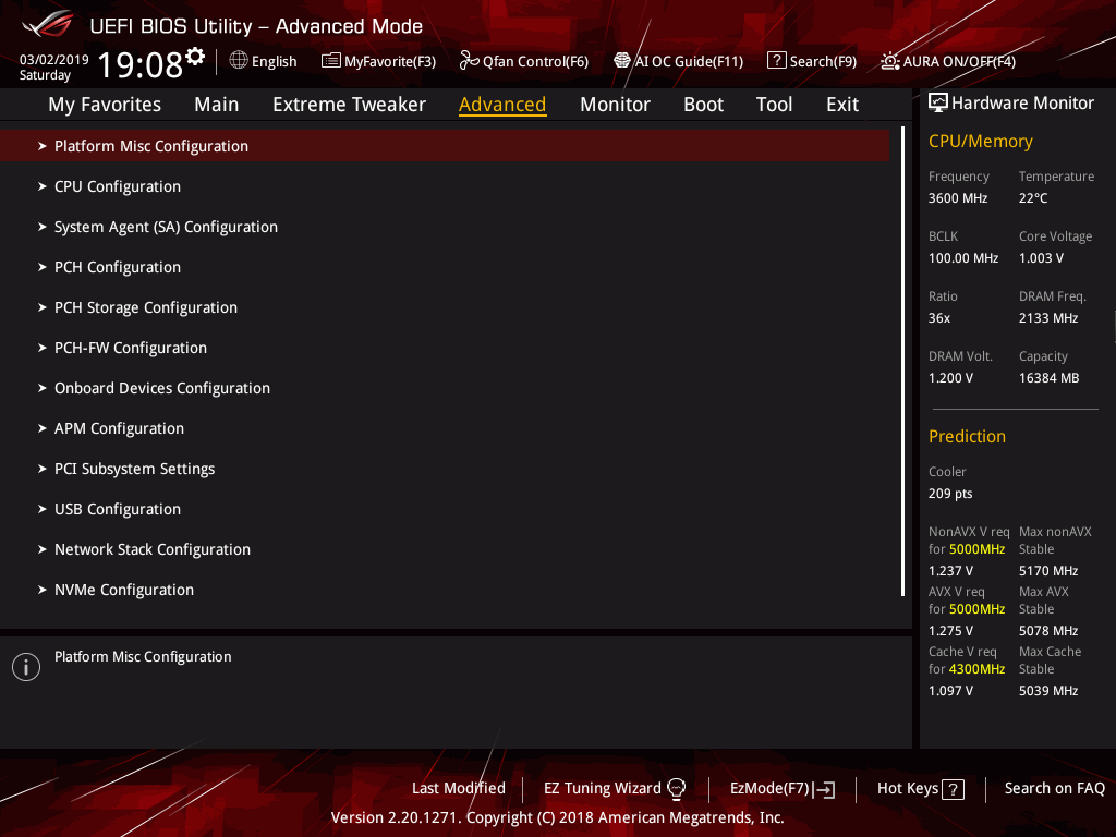
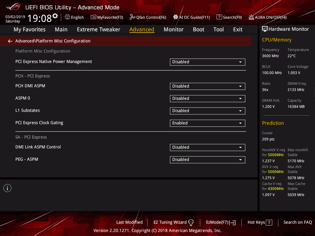
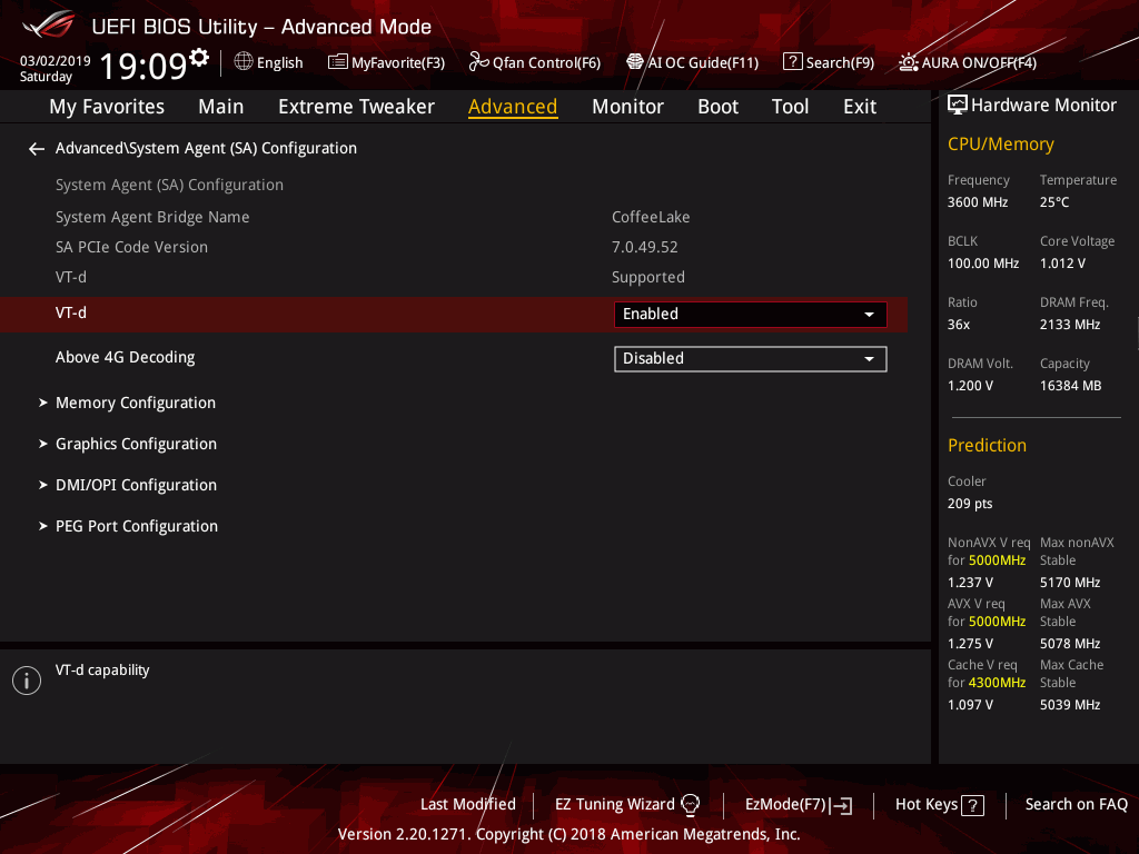
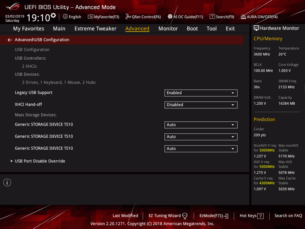
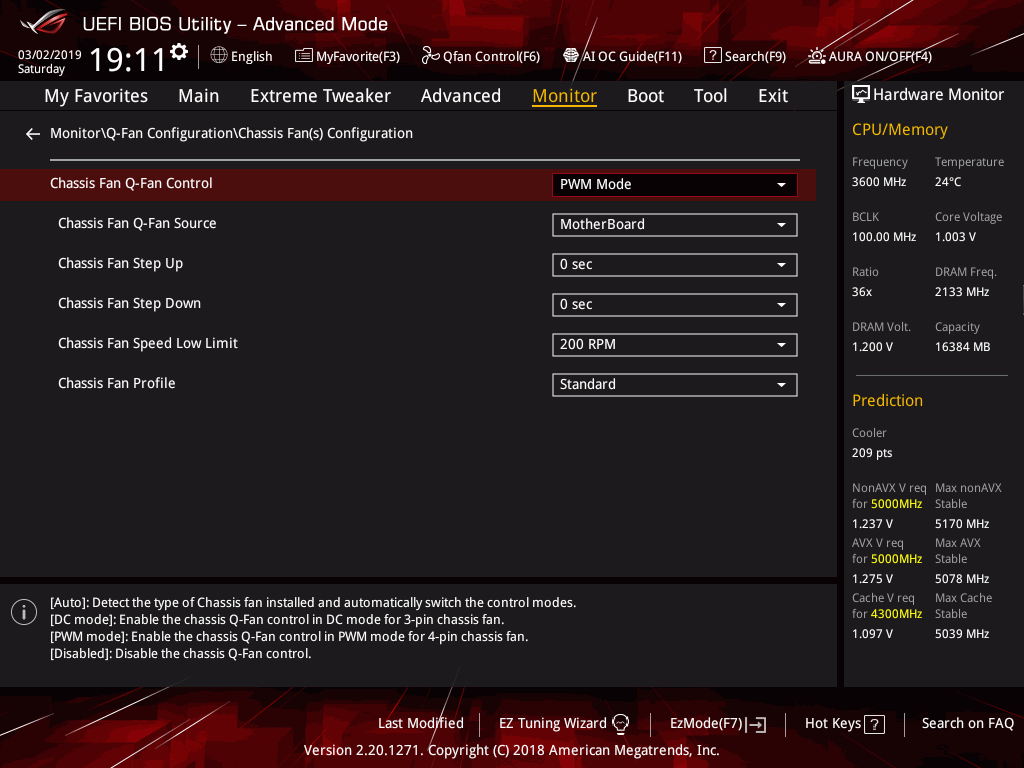
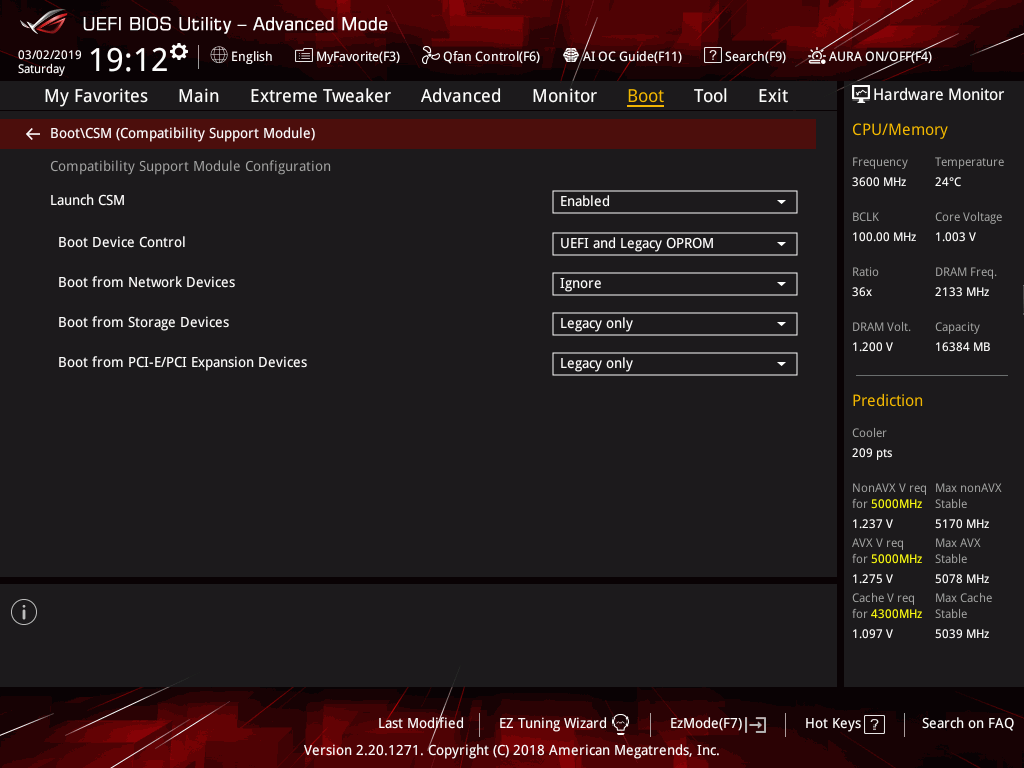
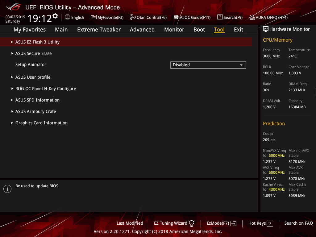
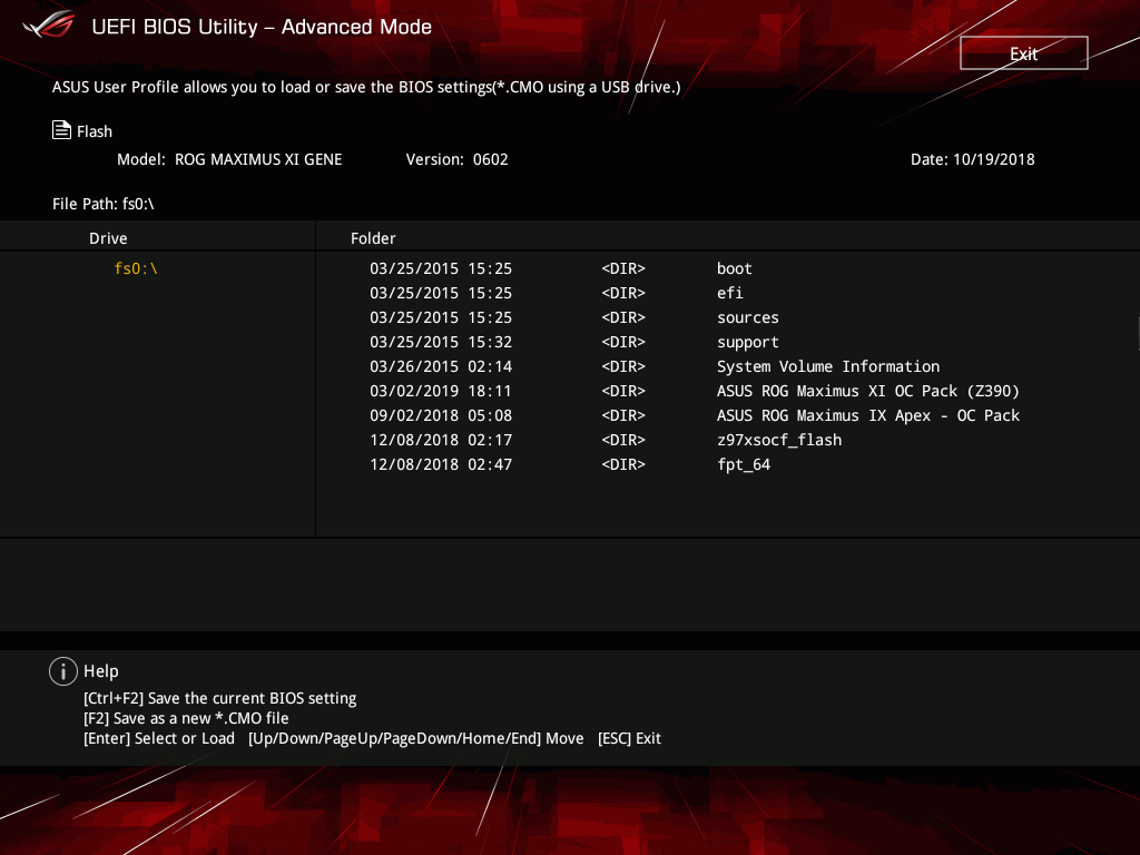
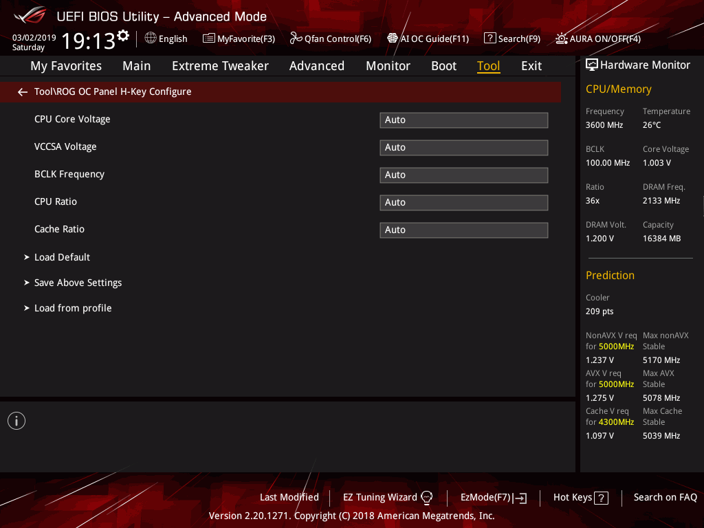
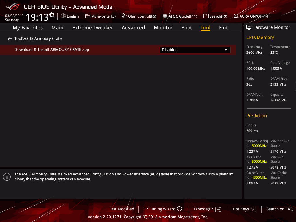
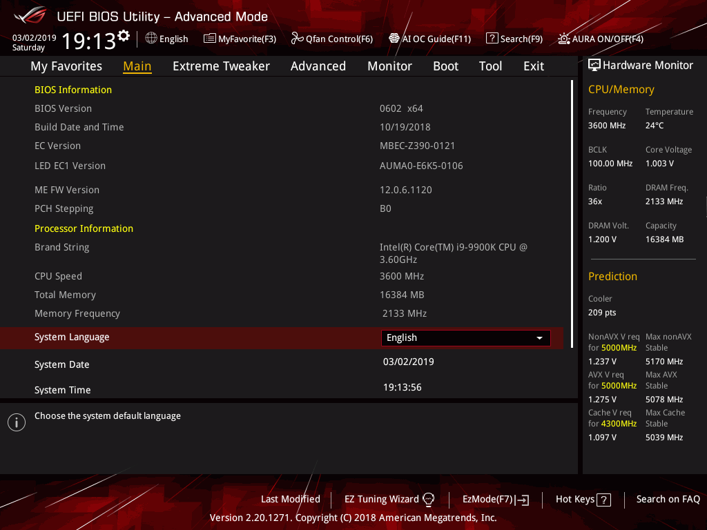
Bilder ( ASUS Maximus XI Gene BIOS walkthrough. - YouTube )


Inoffizielle BIOS Versionen u.a. für Extrem-OC (Achtung: Nutzung auf eigene Gefahr!)
- 0021 (OC BIOS, New Sammy A2 Profiles, need to be logged in @ HWBOT Forums to download)
- 0050 (OC BIOS, allows BCLK change with OC PANEL)
- 0093 (OC BIOS, allow higher voltages without LN2 mode, need to be logged in @ HWBOT Forums to download)
- 0057 (3rd OC BIOS, improves a2 dimms overclocking)
- 0044 (2nd OC BIOS, some memory related fixes vs 0084)
- 0084 (1st OC BIOS for short-traced DIMMs such as G.Skill RGB or Galax based A2-pcb)
News & Reviews
- [Primer] Introducing ROG Maximus and Strix Z390 gaming motherboards for 8-core Intel CPUs | ROG - Republic of Gamers Global
- [Primer] The Z390 motherboard guide: Meet new models from ROG, Strix, TUF Gaming, Prime, and WS
- [Preview] ASUS ROG Z390 Maximus XI Gene Preview | Introduction and Technical Specifications | CPU Mainboard | OC3D Review
- [Review] Tom's Hardware
- [Review] Tech Testers
- [Review] TechGaming
- [Review] HexaTekno
- [Review] GreenTech Reviews
- [Review] Expreview
- [Review] Hardware-Journal
- [Review] Overclock3d.net
- [Review] Overclockers.ua
- [Review] overclockers.ru
- [Review] Bit-Tech.net
- [Review] XFastest
- [Review] ocaholic
- [Review] BenchLife
- [Video-Review] der8auer: ROG Maximus XI Gene Core i9-9900K Overclocking Potenzial - YouTube
Hardwareluxx CPU-Kühler & RAM-Kompatibilitätsliste
1) CPU-Kühler
- Hersteller Modell @ Preisvergleich | Quelle | kompatibel | Einschränkungen / Anmerkungen
- Hersteller Modell @ Preisvergleich | Quelle | inkompatibel | Grund/Foto(s)
- --> Bitte helft mit sammeln!
2) RAM
- Hersteller Modell @ Preisvergleich | Anzahl Module x Größe | Quelle | kompatibel | Einschränkungen / Anmerkungen
- Hersteller Modell @ Preisvergleich | Anzahl Module x Größe | Quelle | inkompatibel | Grund/Screen
- G.SKILL Trident Z F4-3200C15D-32GTZ | 2x16GB | the_patchelor | kompatibel | OC @ DDR4-4133 17-18-18 1.45V & RAM-Tested
- G.SKILL Trident Z F4-3600C17D-16GTZ | 2x8GB | fetzer | kompatibel
- G.SKILL Trident Z F4-4266C19D-16GTZA | 2x8GB | even.de | kompatibel | OC @ DDR4-4500 17-18-18 1.47V & MemTested
- G.SKILL Trident Z F4-4400C19D-16GTZKK | 2x8GB | Low | kompatibel
- G.SKILL Trident Z F4-4500C19D-16GTZKKE | 2x8GB | emissary42 | kompatibel
- G.SKILL Trident Z RGB F4-4133C19D-16GTZR | 2x8GB | aerotracks | kompatibel | OC @ DDR4-4700 18-20-20 1.48V (MemTested)
- G.SKILL Trident Z Royal F4-4000C19D-32GTRS | 2x16GB | emissary42 | kompatibel | momentan nur mit BIOS Versionen bis 0905
- --> Bitte helft mit sammeln!
Wer mir die Arbeit abnehmen möchte, kann seinen Eintrag gern direkt in diesem Format posten. Danke.
Nützliche Links & Tipps (im Forum & im WWW)
1) Hardwareluxx
- [Sammelthread] Intel Coffee Lake RAM OC Thread + Guides und Tipps
- Der offizielle ASUS Support direkt hier im Forum: ASUS
- Direktlink zum ASUS eSupport: per E-Mail & per Telefon
2) WWW (international)
- ASUS ROG Maximus XI @ HWBOT Community Forums
- OC Pack (Download)
enthält:
ROGconnect Plus v1.00.41
TurboV Core v1.03.02
MemTweakIt v2.2.01 - ASMedia USB 3.1 Treiber für Win7 (Download)
3) Tips & Tricks
- RAM OC MemOK per SChalter auf dem Board deaktiiveren beim RAM OC
- ASMedia USB 3(.1) Treiber in das Windows 7 Image integrieren oder P/S2 Tastatur verwenden und die Treiber von einer angeschlossenen Festplatte installieren. Alternativ einen PCIe USB Controller verwenden, der nativ unterstützt wird.
4) FAQ - Frequently Asked Questions
- Q: Wie exakt wird die Vcore per Software ausgelesen?
- A: Elmor hat dies so erklärt:
Elmor schrieb:A note on voltage reporting on the Maximus XI-series, and voltage measurements in general. Like on Crosshair VII Hero, we've improved the SIO voltage readings for better accuracy. The CPU Core Voltage is now reading very close to the voltage the CPU is getting. Applied voltages and load-line levels are comparable to before, but not the software voltage readings.
When measuring voltages on a motherboard and large currents are involved, it's important to use accurate measurement points due to resistance/impedance present on the board. The power plane for example can be modeled as a resistor connected in series between the VRM output and the target device, together with Ohm's law, U = R*I. The larger the current, the larger the voltage drop. If you measure the voltage at the VRM output, for example at the inductor, you'll see a large difference compared to the voltage measured at the CPU socket MLCC. What we're interested in is what voltage the CPU die is actually getting after passing through the output filter, power plane, socket and package.

The Super I/O controller is used by BIOS/AiSuite/CPU-Z/HWInfo/AIDA64 for reading most voltages, temperatures and fan speeds. Its single-ended ADC inputs measure the input voltage referenced to the local SIO ground. With increased VRM output currents, this reading will be more and more inaccurate. We've added a circuit for measuring the differential CPU-die sense and converting it to a single-ended signal to the SIO. The CPU-die sense is accessible through two dedicated pins on the CPU, and are routed to the supply and ground on the CPU die itself. It's typically used by the CPU VRM controller for output voltage control.
Something to look out for is when you're seeing a voltage reported during load which is much higher than what you've set. It would require a negative load-line which is just not supported on any controller as far as I know. At 0 mOhm load-line, you get exactly what you set (Level 8 on M11).
The resulting difference can be seen in the graph below.
Prime95 26.6 12K FFTs

Manual Mode Voltage = Voltage set in BIOS
CPU-die Sense = DMM measurement of the CPU die-sense pins, "true" CPU Core Voltage
Socket MLCC = DMM measurement of the capacitors at the back of the socket
SIO (traditional) = Software reading with standard SIO voltage sense circuit
SIO (Maximus XI Hero) = Software reading with the improved SIO voltage sense circuit
- Q: Das Bluetooth funktionert mit den ASUS Treibern nicht. Gibt es dafür eine Lösung?
- A: Mit den original Intel Treibern v20.70.0.4 gibt es laut Low keine Probleme (Download).
- Q: Meine Tastatur wird beim Systemstart nicht rechtzeitig initialisiert. Wie komme ich ins UEFI?
- A: Die einfachste Möglichkeit ist es, wie im Handbuch beschrieben die Reset Taste dafür zu verwenden. Wer keine Taste mehr dafür an seinem Gehäuse hat, kann auch den Onboard Button verwenden. Für wen weder das Eine noch das Andere in Frage kommt, der kann alternativ auch einen Start ins UEFI mit dem Power Button erzwingen (siehe Handbuch Seite 3-2 "Entering BIOS Setup after POST").
- Q: Wie sind die einzelnen M.2 Steckplätze genau angebunden?
- A: Die beiden auf dem DIMM.2 Modul, teilen sich PCIe Lanes von der CPU mit dem PEG. Wenn das DIMM.2 verwendet wird, reduziert sich dessen Anbindung auf x8. Die beiden Steckpätze auf dem MAinboard selbst sind mit PCIe Lanes vom Chipsatz angebunden. Man hat also die frei Wahl, was einem wichtiger ist (Storage/GPU-Performance).
Anhang anzeigen 457651
- Q: Was ist der Unterschied zwischen XMP-1 und XMP2? Mein Kit sollte eigentlich gar kein zweites XMP besitzen.
- A: ASUS hat den Z390 Modellen eine Funktion spendiert, die statt dem originalen XMP des RAM-Hertellers (XMP-2), von ASUS optmierte Einstellungen verwendet (XMP-1). In der Regel ist XMP-1 zu bevorzugen und etwas performanter, im Fall von Performance- oder Stabilitätsproblemen, empfiehlt es sich aber auf XMP-2 auszuweichen.
Silent Scone@ASUS schrieb:On Z390, there is now the option to use the DIMM profile which is XMP II. These settings are not validated, so mileage will vary depending on the kit and CPU.
XMP I - Board optimised timings
XMP II - Default XMP timings
Often, XMP II timings will be slightly looser depending on the memory kit. If you check within the UEFI or memtweakit, you'll see a difference in memory subsets.
- Q: Wie stelle ich die RTL/IOL richtig ein?
- A: Dazu hat swdtechnik eine Anleitung im Coffee Lake RAM OC Thread gepostet:
Nun wegen RTL`s und IO-L`s und wie man steuern bzw. beeinflussen kann:
wir gehen ins Bios und setzen MRC Fast Boot auf [Disabled]
(wenn Modulen B-Die A2 sind dann zusätzlich noch Trace Centering auf [Enabled])
dann MCH Full Check auf [Enabled]
dazu noch Round Trip Latency auf [Enabled]
noch müssen wir folgende Settings unbedingt auf diese Werte setzen :
DRAM RTL INIT value [x Wert]
DRAM RTL (CHA DIMM0 Rank0) [Auto]
DRAM RTL (CHA DIMM0 Rank1) [Auto]
DRAM RTL (CHA DIMM1 Rank0) [Auto]
DRAM RTL (CHA DIMM1 Rank1) [Auto]
DRAM RTL (CHB DIMM0 Rank0) [Auto]
DRAM RTL (CHB DIMM0 Rank1) [Auto]
DRAM RTL (CHB DIMM1 Rank0) [Auto]
DRAM RTL (CHB DIMM1 Rank1) [Auto]
DRAM IOL (CHA DIMM0 Rank0) [Auto]
DRAM IOL (CHA DIMM0 Rank1) [Auto]
DRAM IOL (CHA DIMM1 Rank0) [Auto]
DRAM IOL (CHA DIMM1 Rank1) [Auto]
DRAM IOL (CHB DIMM0 Rank0) [Auto]
DRAM IOL (CHB DIMM0 Rank1) [Auto]
DRAM IOL (CHB DIMM1 Rank0) [Auto]
DRAM IOL (CHB DIMM1 Rank1) [Auto]
CHA IO_Latency_offset [21]
CHB IO_Latency_offset [21]
CHA RFR delay [14]
CHB RFR delay [14]
den DRAM RTL INIT value [x Wert] rechnen wir mit : (euer tCAS x 2) + IO-L bzw. 4 + IOL Offset bzw. 21 + 10
Jetzt wo alles eingestellt, speichern und Neustarten!
Wenn bootet wieder ins Bios und NUR DRAM RTL INIT value auf eine Zahl runter setzen, speichern und Neustarten!
Und nun so weiter wiederholen mit DRAM RTL INIT value Senkung bis nicht mehr bootet.
Nun haben wir irgendwann Punkt erreicht wo es nicht mehr bootet, dann Power Knopf 5 Sek. lang halten
Rechner geht dann aus.
Wieder Start Knopf drücken, mit F1 ins Bios landen und DRAM RTL INIT value auf den letzten funktionierenden Wert setzen, speichern und Neustarten und ins Windows booten lassen.
So, sind wir im Windows,
Starten nun und ASRock Timing Configurator Programm und schauen auf unsere IO-L´s an!
Die werden im Idealfall gleich sein 7-7 oder 6-6 also, wenn nicht (was am meisten der Fall ist) zbsp. 7-6 oder 6-7 oder 7-13 oder 11-7 oder was auch immer,
dann alles was wir nun brauchen ist nur auf unser Channel A or Channel B, schauen bei dem IOL Wert falsch ist.
Beispiel:
euer letzte ermittelte bootfähige DRAM RTL INIT value Wert ist 68 <---- nur für Beispiel genommene Zahl <---
dabei hat es folgende RTL/IO-L Kombo bei euer DRAM RTL INIT value 68 trainiert
62-63-6-7
aber wir wollen natürlich unsere Werte auf 62-63-6-6 haben
dann alles was wir nun brauchen ist:
ins Bios gehen und unser CHB IO_Latency_offset auf von 21 auf [22] setzen weil genau da unser IO-L nicht stimmt! , speichern und Neustarten.
Nun wird es 62-63-6-6 sein.
Wollen wir mal unser RTL/IO-L Werte beispielweise auf 62-63-5-5 haben
dann gehen wir ins Bios und erhöhen unser DRAM RTL INIT value Wert um eins höher UND NOCH beide CHA IO_Latency_offset / CHB IO_Latency_offset auch um eins höher., nun speichern und Neustarten.
Schon wird es dann 62-63-5-5 sein!
Falls jemand noch Fragen hat, einfach melden")
P.S. - Was aber komisch oder ein Bug von ASRock Timing Configurator Tool ist - manch mal werden die Änderungen von CH IO_Latency_offset im ASRock Timing Configurator Tool nicht angezeigt (oder es ist nur bei mir so das ASRock Tool spinnt), das Asus MemTweakIt dagegen zeigt die Änderungen immer korrekt an (im Reiter "Timings 4" zusehen).
- --> Deine Frage hier!
5) ASUS ROG Wallpaper

6) Wasserkühler (Mainboard)
[Sammelthread] ASUS ROG Maximus XI Apex (90MB0XV0-M0EAY0)
--- Produktseite | PDF-Handbuch | Support-Downloads | Preisvergleich | HWBOT ---
Anhang anzeigen 462223 Anhang anzeigen 462220 Anhang anzeigen 462221 Anhang anzeigen 462222
Anhang anzeigen 462224
Reviews
Inoffizielle BIOS Versionen u.a. für Extrem-OC (Achtung: Nutzung auf eigene Gefahr!)
Dancops ApeXI Guide (Samsung 8Gbit B-Die SR/A2): ROG Maximus XI APEX - NEW BIOS PROFILES small guide @ HWBOT Community Forums
- [Preview] Laurents Choice
- [Preview] IXBT Labs
- [Review] Vmodtech
- [Review] El Chapuzas Informatico
- [Review] Professional Review
- [User Review] chispy @ Xtreme Systems
Inoffizielle BIOS Versionen u.a. für Extrem-OC (Achtung: Nutzung auf eigene Gefahr!)
- 0021 (OC BIOS, New Sammy A2 Profiles)
- 0050 (OC BIOS, allows BCLK change with OC PANEL)
- 0093 (OC BIOS, allows higher voltages without LN2 switch)
- 0033 (early OC BIOS)
Dancops ApeXI Guide (Samsung 8Gbit B-Die SR/A2): ROG Maximus XI APEX - NEW BIOS PROFILES small guide @ HWBOT Community Forums


Zuletzt bearbeitet:
")


