Du verwendest einen veralteten Browser. Es ist möglich, dass diese oder andere Websites nicht korrekt angezeigt werden. Du solltest ein Upgrade durchführen oder einen alternativen Browser verwenden.
ASUS & ASRock sowie MSI? , benutzen ganzzahlige Werte.
Keine Offsets.
Unsicher bei EVGA, Gigabyte und Biostar.
Ein Board welches auf PLLs angesetzt ist, bzw diese nicht selbstständig beim Training korrigiert;
Ist ein fehlerhaftes Board (bzw Bios)
Man geht um das Problem herum, anstelle das Kernproblem herauszufinden.
Wenn es gebraucht wird, wird es gebraucht.
Es macht die Situation jedoch nicht sanfter.
RFC 672 = stepping of 32 ✓
RFCpb 480 = ~50ns under RFC. Alternatively 512 or 544.
CKE, CPDED, XP = surprisingly correct.
Gigabyte FW usually messes that up.
RAS under RCD+X = Invalid for 98%
Under CAS , absolute invalid.
// RAS extends beyond CAS, beyond RCD. On DDR5, SPD-HUB controls association.
Can't open ROW without finding where it is.
Real RAS loaded 70+X.
RCD 49 + RTP (28 invalid value) + ReadBurst (8) + X = 85.
Real RAS loaded/corrected = 105.
tREFi = closest without interrupts 90112(-1) or 98304(-1)
Interface functional value, with interrupts
I have a few questions if I may.
Is it permissible to run the Y Cruncher test at a lower frequency than the normal, daily setting?
I think the daily rate for me is 55p 44e 49r, but I consume too much, so I would prefer to run it at 54p 43e 48r.
I have a rare weak CPU, Vcore demand is huge.
Unfortunately, I haven't been able to make the 8000MHz profile stable since my last post Link, VT3 is failing.
It is only willing to boot with manual ODT, otherwise error 55.
There is no voltage variation at which it boots. It can be imagined that he does not like the cold, the memory is ~8°C. An example in one of your posts, where you specified tXP, tXSR, etc. for an 8000 profile, helped a lot.
On what basis can the values be calculated regularly?
There are plenty of examples on the net, but none of them bring stability to me.
I'm not an expert, long time ago there were many useful descriptions for DDR4, based on them I was able to put together a pretty good one.
There is no DDR5, or I'm blind. I found a lot of useful information here, but I don't think it's enough, or I didn't read it carefully.
The 7200MHz profile is also completely good, with incredibly low voltages, it's great. 7200MHz
From 7600MHz upwards, VT3 is the weak link. 7600MHz TM5 OK Y VT3 error...
If you have a few comments, and you have time, take a look at them.
Just VST is not enough. (VST+VT3 selected for 90+ minutes)
10 loops TM5 1usmus_V3 is not enough.
Thank you for crossquoting
I lost all notifications from 1 week ago.
Still need to process all mentions + requests from 6? , 8 pages ago.
I owe an answer
Been at holiday, it was XMAS ~ let me try to process everything till/before new year.
An example in one of your posts, where you specified tXP, tXSR, etc. for an 8000 profile, helped a lot.
On what basis can the values be calculated regularly?
Half is specifications, half is personal research.
Just maintaining my stuff here and there, when i find motivation.
Was done for me as sanity check. Became useful so i just left it there halfbaked.
Base is ns according to spec. But rounding errors can exist.
Its difficult.
Those voltages are a bit low for 7600.
SA looks ok - IMC is low.
TX then is so so. VCCIO (self generated, is low too)
On 1.45 VDD/Q Mem
You want near 1.3 - 1.32 TX (VDDQ_CPU) for this Boards tuning.
Then because VDD(2)_CPU to VDD_MEM also needs some matching (delta included)
We are looking at near 1.35+. May work with 1.325++, up to Groups.
On that foundation, SA around 1.1 - 1.13 should be fine.
We have to look at values from estimate amperage side, not from the voltage side.
VDD(2)_CPU more is ok, but dont exceed the same VDD_MEM value.
VDDQ_CPU just needs what it needs. RTTs and Groups + RONs influence it, but it appears at least 100mV less than VDDQ_MEM.
To end up around equal matching
At the very end are three things:
~ DQ & DQS need to match at whatever amperage that is. Voltage value irrelevant, its just math.
~ VREF has to be build correctly by the board (i see wonderful Bios progress past me leaving?, OCN) although with zero credit given
~ You need to know your sample , if leaky or not and what voltage ceilings exist. You need to now your board too but first the CPU , to know if it likes or hates voltage.
^ Rest is corrected with PLLs and ODTs. PLLs i would strongly suggest to not touch and leave them alone. Auto is up to FW-Developers intention.
You know i dont trust boards auto values, neither the training most of the times.
VDDQ Training off ~ IF you want torture, and to figure out correct delta.
On , if you are at low clock like now and just copy users settings for trial and error.
Manual labor work , needs real verifications. That means more than 90min y-cruncher. Way more.
We test 6 hours to figure out correct voltages. It is overkill but it is needed, as it will fail between the 2-5 hour mark.
Also das was in asrock steht hab ich eingegeben warum in hwinfo invalide zahlen stehen weiß ich selber nicht muss mal mit Asus schauen und im Bios nochmal kontrollieren
Also das was in asrock steht hab ich eingegeben warum in hwinfo invalide zahlen stehen weiß ich selber nicht muss mal mit Asus schauen und im Bios nochmal kontrollieren
HWInfo hat es korrekt
Der ASRock Timing Configurator/Viewer ist für ASRock Boards gemacht
tWR & WTR sind auslese Fehler.
Manchmal haut er +4 , manchmal +6 oben drauf für nicht ASRock Boards.
MemTweakIT hat je nach Version eine eigenartige Formel für tWR drinnen.
Der Rest wäre korrekt.
Es kann sein, dass es niemand erwähnt hat
Ich verstehe weswegen du die Fehler gemacht hast, aber vieles davon wurde übersehen.
Liegt es an mir ?
DQ RTT WR [40 DRAM Clock]
DQ RTT NOM RD [34 DRAM Clock]
DQ RTT NOM WR [34 DRAM Clock]
DQ RTT PARK [34 DRAM Clock]
DQ RTT PARK DQS [34 DRAM Clock]
GroupA CA ODT [240 DRAM Clock]
GroupA CS ODT [0 DRAM Clock]
GroupA CK ODT [0 DRAM Clock]
GroupB CA ODT [60 DRAM Clock]
GroupB CS ODT [40 DRAM Clock]
GroupB CK ODT [40 DRAM Clock]
Pull-up Output Driver Impedance [34 DRAM Clock]
Pull-Down Output Driver Impedance [34 DRAM Clock]
Reread that
Its not 40ohm for 16gb kits @ very low temp.
RTT + ODT is ok till 55°.
I expect since last 5 Bioses that ASUS FW Team runs better tuning now.
Maybe RTT & ODT are not needed.
I want 80° mem stability, but oh well.
No DDR5 system, to work on any further.
EDIT:
You know what,
On old Bios you can just use my Biosmod till 8400, to have all memory tuning options;
Or go with 0080 (if it exists) for white APEX.
I'm in no hurry, please enjoy the holidays.
I read the useful tips, I use what I understand from them.
That's why I bought it, I want to learn more about how DDR5 works. I have another small machine, a z590/RKL, which I use.
I bought it ~2 months ago, and my plan is to take the frequencies in small steps (400MHz) as long as it works.
I started at 5600, then 6000, 6400, 6800, 7200, and now 7600 but with errors.
Even before, but I was able to stabilize them by looking for voltage.
Here now, if I increase it, it gets worse. I would, but unfortunately it doesn't help. I see other people's values, they are immediately wrong.
In any case, I will continue, I will not give up, I will not jump to 8000, because 7600 is not stable yet.
Sometimes I will share MemTweak windows + hwinfo here.
I don't read OCN, it's too fast for me.
Thank you for the useful tips, I will remain a reader in the background, I will use many things.
Now the 7600 will continue as time permits.
Regards, zeb
Edit:
Sorry, gaved too much info.
BIOS settings is my 8000 profil. I used correct ctl's, noticed all data
Now I will stop the 8000MHz, i don't wanna mix. Later.
Sometimes hard, in hungarian forum every member only 8000+ profiles... i don't care.
Die 7 bei TRDRD_dg und TWRWR_dg werden keine Fehlerquellen sein bei Testmem5, die werden aufgerundet. Sprich die 7 war schon eine 8. Aus einer 9 würde ebenfalls eine 10 werden usw..
Die 7 bei TRDRD_dg und TWRWR_dg werden keine Fehlerquellen sein bei Testmem5, die werden aufgerundet. Sprich die 7 war schon eine 8. Aus einer 9 würde ebenfalls eine 10 werden usw..
Brauche mal noch etwas Input zu meinen Einstellungen. RAM läuft auf 7600MHz, mehr ist nicht möglich. Die CPU ist zu schwach, Board/RAM Technisch ja, CPU IMC aber nein. Es sei denn ich erhalte hier noch spezielle Tipps.
I pushed the 7600 profile quickly after work.
I'm late, I see I'm not alone. Unfortunately, I noticed it too late, so I can show you the current setup.
A record, since it never went for 10 minutes. I know 10 minutes is very weak. Unfortunately, that's all I could fit in, I have to sleep. I'll get up right away...
VDDQ Training Disabled, Tx and MC Voltage are more. ODTs, too.
[2023/12/26 07:49:20]
Ai Overclock Tuner [Auto]
Intel(R) Adaptive Boost Technology [Auto]
ASUS MultiCore Enhancement [Auto – Lets BIOS Optimize]
SVID Behavior [Auto]
BCLK Frequency : DRAM Frequency Ratio [100:100]
Memory Controller : DRAM Frequency Ratio [1:2]
DRAM Frequency [DDR5-7600MHz]
Performance Core Ratio [By Core Usage]
1-Core Ratio Limit [57]
2-Core Ratio Limit [57]
3-Core Ratio Limit [56]
4-Core Ratio Limit [56]
5-Core Ratio Limit [55]
6-Core Ratio Limit [55]
7-Core Ratio Limit [54]
8-Core Ratio Limit [54]
Performance Core0 Specific Ratio Limit [Auto]
Performance Core0 specific Voltage [Auto]
Performance Core1 Specific Ratio Limit [Auto]
Performance Core1 specific Voltage [Auto]
*Performance Core2 Specific Ratio Limit [Auto]
Performance Core2 specific Voltage [Auto]
*Performance Core3 Specific Ratio Limit [Auto]
Performance Core3 specific Voltage [Auto]
Performance Core4 Specific Ratio Limit [Auto]
Performance Core4 specific Voltage [Auto]
Performance Core5 Specific Ratio Limit [Auto]
Performance Core5 specific Voltage [Auto]
Performance Core6 Specific Ratio Limit [Auto]
Performance Core6 specific Voltage [Auto]
Performance Core7 Specific Ratio Limit [Auto]
Performance Core7 specific Voltage [Auto]
Efficient Core Ratio [By Core Usage]
Efficient Turbo Ratio Limit 1 [43]
Efficient Turbo Ratio Cores 1 [Auto]
Efficient Core Group0 Specific Ratio Limit [45]
Efficient Core Group0 specific Voltage [Auto]
Efficient Core Group1 Specific Ratio Limit [45]
Efficient Core Group1 specific Voltage [Auto]
Efficient Core Group2 Specific Ratio Limit [45]
Efficient Core Group2 specific Voltage [Auto]
Efficient Core Group3 Specific Ratio Limit [45]
Efficient Core Group3 specific Voltage [Auto]
AVX2 [Enabled]
AVX2 Ratio Offset to per-core Ratio Limit [User Specify]
AVX2 Ratio Offset [0]
AVX2 Voltage Guardband Scale Factor [User Specify]
AVX2 Voltage Guardband Scale Factor [0]
Maximus Tweak [Mode 2]
DRAM CAS# Latency [34]
DRAM RAS# to CAS# Delay Read [44]
DRAM RAS# to CAS# Delay Write [14]
DRAM RAS# PRE Time [44]
DRAM RAS# ACT Time [56]
DRAM Command Rate [2N]
DRAM RAS# to RAS# Delay L [12]
DRAM RAS# to RAS# Delay S [8]
DRAM REF Cycle Time 2 [480]
DRAM REF Cycle Time Same Bank [Auto]
DRAM Refresh Interval [131071]
DRAM WRITE Recovery Time [Auto]
DRAM READ to PRE Time [12]
DRAM FOUR ACT WIN Time [32]
DRAM WRITE to READ Delay L [18]
DRAM WRITE to READ Delay S [8]
DRAM CKE Minimum Pulse Width [Auto]
DRAM Write Latency [32]
Ctl0 dqvrefup [162]
Ctl0 dqvrefdn [80]
Ctl0 dqodtvrefup [Auto]
Ctl0 dqodtvrefdn [Auto]
Ctl1 cmdvrefup [Auto]
Ctl1 ctlvrefup [Auto]
Ctl1 clkvrefup [Auto]
Ctl1 ckecsvrefup [Auto]
Ctl2 cmdvrefdn [Auto]
Ctl2 ctlvrefdn [Auto]
Ctl2 clkvrefdn [Auto]
Read Equalization RxEq Start Sign [-]
Read Equalization RxEq Start [Auto]
Read Equalization RxEq Stop Sign [-]
Read Equalization RxEq Stop [Auto]
ODT_READ_DURATION [Auto]
ODT_READ_DELAY [Auto]
ODT_WRITE_DURATION [Auto]
ODT_WRITE_DELAY [Auto]
DQ RTT WR [40 DRAM Clock]
DQ RTT NOM RD [40 DRAM Clock]
DQ RTT NOM WR [40 DRAM Clock]
DQ RTT PARK [34 DRAM Clock]
DQ RTT PARK DQS [34 DRAM Clock]
GroupA CA ODT [240 DRAM Clock]
GroupA CS ODT [0 DRAM Clock]
GroupA CK ODT [0 DRAM Clock]
GroupB CA ODT [60 DRAM Clock]
GroupB CS ODT [40 DRAM Clock]
GroupB CK ODT [40 DRAM Clock]
Pull-up Output Driver Impedance [34 DRAM Clock]
Pull-Down Output Driver Impedance [34 DRAM Clock]
Round Trip Latency Init Value MC0 CHA [Auto]
Round Trip Latency Max Value MC0 CHA [Auto]
Round Trip Latency Offset Value Mode Sign MC0 CHA [-]
Round Trip Latency Offset Value MC0 CHA [Auto]
Round Trip Latency Init Value MC0 CHB [Auto]
Round Trip Latency Max Value MC0 CHB [Auto]
Round Trip Latency Offset Value Mode Sign MC0 CHB [-]
Round Trip Latency Offset Value MC0 CHB [Auto]
Round Trip Latency Init Value MC1 CHA [Auto]
Round Trip Latency Max Value MC1 CHA [Auto]
Round Trip Latency Offset Value Mode Sign MC1 CHA [-]
Round Trip Latency Offset Value MC1 CHA [Auto]
Round Trip Latency Init Value MC1 CHB [Auto]
Round Trip Latency Max Value MC1 CHB [Auto]
Round Trip Latency Offset Value Mode Sign MC1 CHB [-]
Round Trip Latency Offset Value MC1 CHB [Auto]
Round Trip Latency MC0 CHA R0 [Auto]
Round Trip Latency MC0 CHA R1 [Auto]
Round Trip Latency MC0 CHA R2 [0]
Round Trip Latency MC0 CHA R3 [0]
Round Trip Latency MC0 CHA R4 [0]
Round Trip Latency MC0 CHA R5 [0]
Round Trip Latency MC0 CHA R6 [0]
Round Trip Latency MC0 CHA R7 [0]
Round Trip Latency MC0 CHB R0 [Auto]
Round Trip Latency MC0 CHB R1 [Auto]
Round Trip Latency MC0 CHB R2 [0]
Round Trip Latency MC0 CHB R3 [0]
Round Trip Latency MC0 CHB R4 [0]
Round Trip Latency MC0 CHB R5 [0]
Round Trip Latency MC0 CHB R6 [0]
Round Trip Latency MC0 CHB R7 [0]
Round Trip Latency MC1 CHA R0 [Auto]
Round Trip Latency MC1 CHA R1 [Auto]
Round Trip Latency MC1 CHA R2 [0]
Round Trip Latency MC1 CHA R3 [0]
Round Trip Latency MC1 CHA R4 [0]
Round Trip Latency MC1 CHA R5 [0]
Round Trip Latency MC1 CHA R6 [0]
Round Trip Latency MC1 CHA R7 [0]
Round Trip Latency MC1 CHB R0 [Auto]
Round Trip Latency MC1 CHB R1 [Auto]
Round Trip Latency MC1 CHB R2 [0]
Round Trip Latency MC1 CHB R3 [0]
Round Trip Latency MC1 CHB R4 [0]
Round Trip Latency MC1 CHB R5 [0]
Round Trip Latency MC1 CHB R6 [0]
Round Trip Latency MC1 CHB R7 [0]
Early Command Training [Auto]
SenseAmp Offset Training [Auto]
Early ReadMPR Timing Centering 2D [Auto]
Read MPR Training [Auto]
Receive Enable Training [Auto]
Jedec Write Leveling [Auto]
Early Write Time Centering 2D [Auto]
Early Read Time Centering 2D [Auto]
Write Timing Centering 1D [Auto]
Write Voltage Centering 1D [Auto]
Read Timing Centering 1D [Auto]
Read Timing Centering with JR [Auto]
Dimm ODT Training* [Disabled]
Max RTT_WR [ODT Off]
DIMM RON Training* [Auto]
Write Drive Strength/Equalization 2D* [Auto]
Write Slew Rate Training* [Auto]
Read ODT Training* [Auto]
Comp Optimization Training [Auto]
Read Equalization Training* [Auto]
Read Amplifier Training* [Auto]
Write Timing Centering 2D [Auto]
Read Timing Centering 2D [Auto]
Command Voltage Centering [Auto]
Early Command Voltage Centering [Auto]
Write Voltage Centering 2D [Auto]
Read Voltage Centering 2D [Auto]
Late Command Training [Auto]
Round Trip Latency [Enabled]
Turn Around Timing Training [Auto]
CMD CTL CLK Slew Rate [Auto]
CMD/CTL DS & E 2D [Auto]
Read Voltage Centering 1D [Auto]
TxDqTCO Comp Training* [Auto]
ClkTCO Comp Training* [Auto]
TxDqsTCO Comp Training* [Auto]
VccDLL Bypass Training [Auto]
CMD/CTL Drive Strength Up/Dn 2D [Auto]
DIMM CA ODT Training [Auto]
PanicVttDnLp Training* [Auto]
Read Vref Decap Training* [Auto]
Vddq Training [Disabled]
Duty Cycle Correction Training [Auto]
Periodic DCC [Auto]
Rank Margin Tool Per Bit [Auto]
DIMM DFE Training [Auto]
EARLY DIMM DFE Training [Auto]
Tx Dqs Dcc Training [Auto]
DRAM DCA Training [Auto]
Write Driver Strength Training [Auto]
Rank Margin Tool [Auto]
Memory Test [Auto]
DIMM SPD Alias Test [Auto]
Receive Enable Centering 1D [Auto]
Retrain Margin Check [Auto]
Write Drive Strength Up/Dn independently [Auto]
LPDDR DqDqs Re-Training [Auto]
Margin Check Limit [Disabled]
tRDRD_sg_Training [Auto]
tRDRD_sg_Runtime [16]
tRDRD_dg_Training [Auto]
tRDRD_dg_Runtime [8]
tRDWR_sg [20]
tRDWR_dg [20]
tWRWR_sg [16]
tWRWR_dg [8]
tWRRD_sg [Auto]
tWRRD_dg [Auto]
tRDRD_dr [0]
tRDRD_dd [Auto]
tRDWR_dr [0]
tRDWR_dd [Auto]
tWRWR_dr [0]
tWRWR_dd [Auto]
tWRRD_dr [0]
tWRRD_dd [Auto]
tRPRE [Auto]
tWPRE [Auto]
tWPOST [Auto]
tWRPRE [60]
tPRPDEN [Auto]
tRDPDEN [Auto]
tWRPDEN [61]
tCPDED [Auto]
tREFIX9 [Auto]
Ref Interval [Auto]
tXPDLL [Auto]
tXP [Auto]
tPPD [Auto]
tCCD_L_tDLLK [Auto]
tZQCAL [Auto]
tZQCS [Auto]
OREF_RI [Auto]
Refresh Watermarks [High]
Refresh Hp Wm [Auto]
Refresh Panic Wm [Auto]
Refresh Abr Release [Auto]
tXSDLL [Auto]
tZQOPER [Auto]
tMOD [Auto]
CounttREFIWhileRefEn [Auto]
HPRefOnMRS [Auto]
SRX Ref Debits [Auto]
RAISE BLK WAIT [Auto]
Ref Stagger En [Auto]
Ref Stagger Mode [Auto]
Disable Stolen Refresh [Auto]
En Ref Type Display [Auto]
Trefipulse Stagger Disable [Auto]
tRPab ext [Auto]
derating ext [Auto]
Allow 2cyc B2B LPDDR [Auto]
tCSH [Auto]
tCSL [Auto]
powerdown Enable [Auto]
idle length [Auto]
raise cke after exit latency [Auto]
powerdown latency [Auto]
powerdown length [Auto]
selfrefresh latency [Auto]
selfrefresh length [Auto]
ckevalid length [Auto]
ckevalid enable [Auto]
idle enable [Auto]
selfrefresh enable [Auto]
Address mirror [Auto]
no gear4 param divide [Auto]
x8 device [Auto]
no gear2 param divide [Auto]
ddr 1dpc split ranks on subch [Auto]
write0 enable [Auto]
MultiCycCmd [Auto]
WCKDiffLowInIdle [Auto]
PBR Disable [Auto]
PBR OOO Dis [Auto]
PBR Disable on hot [Auto]
PBR Exit on Idle Cnt [Auto]
tXSR [Auto]
Dec tCWL [Auto]
Add tCWL [Auto]
Add 1Qclk delay [Auto]
MRC Fast Boot [Disabled]
MCH Full Check [Enabled]
Mem Over Clock Fail Count [2]
Training Profile [Auto]
RxDfe [Auto]
Mrc Training Loop Count [2]
DRAM CLK Period [Auto]
Dll_bwsel [Auto]
Controller 0, Channel 0 Control [Enabled]
Controller 0, Channel 1 Control [Enabled]
Controller 1, Channel 0 Control [Enabled]
Controller 1, Channel 1 Control [Enabled]
MC_Vref0 [Auto]
MC_Vref1 [Auto]
MC_Vref2 [Auto]
Fine Granularity Refresh mode [Auto]
SDRAM Density Per Die [Auto]
SDRAM Banks Per Bank Group [Auto]
SDRAM Bank Groups [Auto]
Dynamic Memory Boost [Disabled]
Realtime Memory Frequency [Disabled]
SA GV [Disabled]
Voltage Monitor [Die Sense]
VRM Initialization Check [Enabled]
CPU Input Voltage Load-line Calibration [Auto]
CPU Load-line Calibration [Level 5]
Synch ACDC Loadline with VRM Loadline [Disabled]
CPU Current Capability [Auto]
CPU Current Reporting [Auto]
Core Voltage Suspension [Auto]
CPU VRM Switching Frequency [Manual]
Fixed CPU VRM Switching Frequency(KHz) [300]
CPU Power Duty Control [T.Probe]
CPU Power Phase Control [Optimized]
CPU Power Thermal Control [125]
CPU Core/Cache Boot Voltage [Auto]
CPU Input Boot Voltage [Auto]
PLL Termination Boot Voltage [Auto]
CPU Standby Boot Voltage [Auto]
Memory Controller Boot Voltage [Auto]
CPU Core Auto Voltage Cap [Auto]
CPU Input Auto Voltage Cap [Auto]
Memory Controller Auto Voltage Cap [Auto]
Maximum CPU Core Temperature [85]
Fast Throttle Threshold [Auto]
Package Temperature Threshold [Auto]
Regulate Frequency by above Threshold [Auto]
IVR Transmitter VDDQ ICCMAX [Auto]
Unlimited ICCMAX [Auto]
CPU Core/Cache Current Limit Max. [Auto]
Long Duration Package Power Limit [255]
Package Power Time Window [Auto]
Short Duration Package Power Limit [270]
Dual Tau Boost [Disabled]
IA AC Load Line [0.01]
IA DC Load Line [0.84]
IA CEP Enable [Auto]
SA CEP Enable [Auto]
IA SoC Iccmax Reactive Protector [Auto]
Inverse Temperature Dependency Throttle [Auto]
IA VR Voltage Limit [1500]
CPU SVID Support [Auto]
Cache Dynamic OC Switcher [Disabled]
TVB Voltage Optimizations [Disabled]
Enhanced TVB [Disabled]
Overclocking TVB [Disabled]
Overclocking TVB Global Temperature Offset Sign [+]
Overclocking TVB Global Temperature Offset Value [Auto]
Offset Mode Sign 1 [+]
V/F Point 1 Offset [Auto]
Offset Mode Sign 2 [+]
V/F Point 2 Offset [Auto]
Offset Mode Sign 3 [+]
V/F Point 3 Offset [Auto]
Offset Mode Sign 4 [+]
V/F Point 4 Offset [Auto]
Offset Mode Sign 5 [+]
V/F Point 5 Offset [Auto]
Offset Mode Sign 6 [+]
V/F Point 6 Offset [Auto]
Offset Mode Sign 7 [+]
V/F Point 7 Offset [Auto]
Offset Mode Sign 8 [+]
V/F Point 8 Offset [Auto]
Offset Mode Sign 9 [+]
V/F Point 9 Offset [Auto]
Offset Mode Sign 10 [+]
V/F Point 10 Offset [Auto]
Offset Mode Sign 11 [+]
V/F Point 11 Offset [Auto]
Initial BCLK Frequency [Auto]
Runtime BCLK OC [Auto]
BCLK Amplitude [Auto]
BCLK Slew Rate [Auto]
BCLK Spread Spectrum [Auto]
Initial PCIE Frequency [Auto]
PCIE/DMI Amplitude [Auto]
PCIE/DMI Slew Rate [Auto]
PCIE/DMI Spread Spectrum [Auto]
Cold Boot PCIE Frequency [Auto]
Realtime Memory Timing [Disabled]
SPD Write Disable [TRUE]
PVD Ratio Threshold [Auto]
SA PLL Frequency Override [Auto]
BCLK TSC HW Fixup [Enabled]
Core Ratio Extension Mode [Disabled]
FLL OC mode [Auto]
UnderVolt Protection [Disabled]
Switch Microcode [Current Microcode]
Xtreme Tweaking [Disabled]
Core PLL Voltage [Auto]
GT PLL Voltage [Auto]
Ring PLL Voltage [Auto]
System Agent PLL Voltage [Auto]
Memory Controller PLL Voltage [Auto]
Efficient-core PLL Voltage [Auto]
CPU 1.8V Small Rail [Auto]
PLL Termination Voltage [Auto]
CPU Standby Voltage [Auto]
PCH 1.05V Voltage [Auto]
PCH 0.82V Voltage [Auto]
CPU Input Voltage Reset Voltage [Auto]
Eventual CPU Input Voltage [Auto]
Eventual Memory Controller Voltage [Auto]
Package Temperature Threshold [Auto]
Regulate Frequency by above Threshold [Auto]
Cooler Efficiency Customize [Keep Training]
Cooler Re-evaluation Algorithm [Normal]
Optimism Scale [100]
Ring Down Bin [Auto]
Min. CPU Cache Ratio [Auto]
Max. CPU Cache Ratio [48]
BCLK Aware Adaptive Voltage [Auto]
Actual VRM Core Voltage [Auto]
Global Core SVID Voltage [Adaptive Mode]
- Offset Mode Sign [-]
- Additional Turbo Mode CPU Core Voltage [Auto]
- Offset Voltage [0.08000]
Cache SVID Voltage [Adaptive Mode]
- Offset Mode Sign [-]
- Additional Turbo Mode Cache Voltage [Auto]
- Offset Voltage [0.02000]
CPU L2 Voltage [Adaptive Mode]
- Offset Mode Sign [-]
- Additional Turbo Mode CPU L2 Voltage [Auto]
- Offset Voltage [0.02000]
CPU System Agent Voltage [Manual Mode]
- CPU System Agent Voltage Override [1.12000]
CPU Input Voltage [Auto]
High DRAM Voltage Mode [Enabled]
DRAM VDD Voltage [1.44000]
DRAM VDDQ Voltage [1.42000]
IVR Transmitter VDDQ Voltage [1.30000]
Memory Controller Voltage [1.36250]
MC Voltage Calculation Voltage Base [Auto]
VDD Calculation Voltage Base [Auto]
PMIC Voltages [Auto]
PCI Express Native Power Management [Enabled]
Native ASPM [Disabled]
DMI Link ASPM Control [Disabled]
ASPM [Auto]
L1 Substates [Disabled]
DMI ASPM [Disabled]
DMI Gen3 ASPM [Disabled]
PEG - ASPM [Disabled]
PCI Express Clock Gating [Enabled]
Hardware Prefetcher [Enabled]
Adjacent Cache Line Prefetch [Enabled]
Intel (VMX) Virtualization Technology [Disabled]
Per P-Core Control [Disabled]
Per E-Core Control [Disabled]
Active Performance Cores [All]
Active Efficient Cores [All]
Hyper-Threading [Enabled]
Hyper-Threading of Core 0 [Enabled]
Hyper-Threading of Core 1 [Enabled]
Hyper-Threading of Core 2 [Enabled]
Hyper-Threading of Core 3 [Enabled]
Hyper-Threading of Core 4 [Enabled]
Hyper-Threading of Core 5 [Enabled]
Hyper-Threading of Core 6 [Enabled]
Hyper-Threading of Core 7 [Enabled]
Total Memory Encryption [Disabled]
Legacy Game Compatibility Mode [Disabled]
Boot performance mode [Auto]
Intel(R) SpeedStep(tm) [Enabled]
Intel(R) Speed Shift Technology [Disabled]
Turbo Mode [Enabled]
Acoustic Noise Mitigation [Disabled]
CPU C-states [Auto]
Thermal Monitor [Enabled]
Dual Tau Boost [Disabled]
VT-d [Disabled]
Memory Remap [Enabled]
Enable VMD controller [Enabled]
Map PCIE Storage under VMD [Disabled]
Map SATA Controller under VMD [Disabled]
M.2_1 Link Speed [Auto]
PCIEX16(G5)_1 Link Speed [Auto]
PCIEX16(G5)_2 Link Speed [Auto]
PCIEX1(G4) Link Speed [Auto]
PCIEX4(G4) Link Speed [Auto]
M.2_2 Link Speed [Auto]
DIMM.2_1 Link Speed [Auto]
DIMM.2_2 Link Speed [Auto]
SATA Controller(s) [Enabled]
Aggressive LPM Support [Disabled]
SMART Self Test [Enabled]
M.2_3 [Enabled]
M.2_3 Hot Plug [Disabled]
SATA6G_1 [Enabled]
SATA6G_1 Hot Plug [Disabled]
SATA6G_2 [Enabled]
SATA6G_2 Hot Plug [Disabled]
SATA6G_3 [Enabled]
SATA6G_3 Hot Plug [Disabled]
SATA6G_4 [Enabled]
SATA6G_4 Hot Plug [Disabled]
PTT [Enable]
Intel(R) Dynamic Tuning Technology [Disabled]
PCIE Tunneling over USB4 [Enabled]
Discrete Thunderbolt(TM) Support [Disabled]
Security Device Support [Enable]
SHA256 PCR Bank [Enabled]
Pending operation [None]
Platform Hierarchy [Enabled]
Storage Hierarchy [Enabled]
Endorsement Hierarchy [Enabled]
Physical Presence Spec Version [1.3]
Disable Block Sid [Disabled]
Password protection of Runtime Variables [Enable]
Above 4G Decoding [Enabled]
Resize BAR Support [Enabled]
SR-IOV Support [Disabled]
Legacy USB Support [Enabled]
XHCI Hand-off [Enabled]
SanDisk [Auto]
LAN_U32G2_1 [Enabled]
U32G1_E5 [Enabled]
U32G1_E6 [Enabled]
U32G1_E7 [Enabled]
U32G1_E8 [Enabled]
U32G2X2_C3 [Enabled]
U32G2_5 [Enabled]
U32G2_6 [Enabled]
U32G2_7 [Enabled]
U32G2_P8 [Enabled]
U32G2X2_C9 [Enabled]
U32G1_E1 [Enabled]
U32G1_E2 [Enabled]
U32G1_E3 [Enabled]
U32G1_E4 [Enabled]
Network Stack [Disabled]
Device [N/A]
Restore AC Power Loss [Power Off]
Max Power Saving [Disabled]
ErP Ready [Disabled]
Power On By PCI-E [Disabled]
Power On By RTC [Disabled]
USB Audio [Enabled]
Intel LAN [Enabled]
USB power delivery in Soft Off state (S5) [Disabled]
Connectivity mode (Wi-Fi & Bluetooth) [Disabled]
When system is in working state [All On]
Q-Code LED Function [POST Code Only]
When system is in sleep, hibernate or soft off states [All On]
M.2_2 Configuration [Auto]
ASMedia USB 3.2 Controller_U32G1_E12 [Enabled]
ASMedia USB 3.2 Controller_U32G1_E34 [Enabled]
GNA Device [Disabled]
ASMedia Storage Controller [Enabled]
Windows Hot-plug Notification [Disabled]
ASPM Support [Disabled]
CPU Temperature [Monitor]
CPU Package Temperature [Monitor]
MotherBoard Temperature [Monitor]
VRM Temperature [Monitor]
Chipset Temperature [Monitor]
T_Sensor Temperature [Monitor]
DIMM.2 Sensor 1 Temperature [Monitor]
DIMM.2 Sensor 2 Temperature [Monitor]
Water In T Sensor Temperature [Monitor]
Water Out T Sensor Temperature [Monitor]
DIMM A1 Temperature [Monitor]
DIMM B1 Temperature [Monitor]
CPU Fan Speed [Monitor]
CPU Optional Fan Speed [Monitor]
Chassis Fan 1 Speed [Monitor]
Chassis Fan 2 Speed [Monitor]
Chassis Fan 3 Speed [Monitor]
Water Pump+ Speed [Monitor]
AIO Pump Speed [Monitor]
Flow Rate [Monitor]
CPU Core Voltage [Monitor]
12V Voltage [Monitor]
5V Voltage [Monitor]
3.3V Voltage [Monitor]
Memory Controller Voltage [Monitor]
CPU Fan Q-Fan Control [DC Mode]
CPU Fan Profile [Standard]
CPU Fan Q-Fan Source [CPU]
CPU Fan Step Up [Level 0]
CPU Fan Step Down [Level 4]
CPU Fan Speed Low Limit [200 RPM]
Chassis Fan 1 Q-Fan Control [Auto Detect]
Chassis Fan 1 Profile [Standard]
Chassis Fan 1 Q-Fan Source [CPU]
Chassis Fan 1 Step Up [Level 0]
Chassis Fan 1 Step Down [Level 0]
Chassis Fan 1 Speed Low Limit [200 RPM]
Chassis Fan 2 Q-Fan Control [PWM Mode]
Chassis Fan 2 Profile [Standard]
Chassis Fan 2 Q-Fan Source [Chipset]
Chassis Fan 2 Step Up [Level 0]
Chassis Fan 2 Step Down [Level 4]
Chassis Fan 2 Speed Low Limit [200 RPM]
Chassis Fan 3 Q-Fan Control [DC Mode]
Chassis Fan 3 Profile [Silent]
Chassis Fan 3 Q-Fan Source [CPU]
Chassis Fan 3 Step Up [Level 0]
Chassis Fan 3 Step Down [Level 0]
Chassis Fan 3 Speed Low Limit [200 RPM]
Water Pump+ Q-Fan Control [PWM Mode]
Water Pump+ Profile [Manual]
Water Pump+ Q-Fan Source [CPU]
Water Pump+ Step Up [Level 0]
Water Pump+ Step Down [Level 4]
Water Pump+ Speed Low Limit [Ignore]
Water Pump+ Point4 Temperature [70]
Water Pump+ Point4 Duty Cycle (%) [100]
Water Pump+ Point3 Temperature [50]
Water Pump+ Point3 Duty Cycle (%) [85]
Water Pump+ Point2 Temperature [40]
Water Pump+ Point2 Duty Cycle (%) [80]
Water Pump+ Point1 Temperature [25]
Water Pump+ Point1 Duty Cycle (%) [60]
AIO Pump Q-Fan Control [Auto Detect]
AIO Pump Profile [Full Speed]
CPU Temperature LED Switch [Enabled]
Launch CSM [Disabled]
OS Type [Other OS]
Secure Boot Mode [Custom]
Fast Boot [Enabled]
Next Boot after AC Power Loss [Fast Boot]
Boot Logo Display [Disabled]
POST Report [5 sec]
Bootup NumLock State [On]
Wait For 'F1' If Error [Enabled]
Option ROM Messages [Force BIOS]
Interrupt 19 Capture [Disabled]
AMI Native NVMe Driver Support [Enabled]
Setup Mode [Advanced Mode]
Boot Sector (MBR/GPT) Recovery Policy [Local User Control]
Next Boot Recovery Action [Skip]
BIOS Image Rollback Support [Enabled]
Publish HII Resources [Disabled]
Flexkey [Safe Boot]
Setup Animator [Disabled]
Load from Profile [5]
Profile Name [7600CL34*44*44]
Save to Profile [5]
DIMM Slot Number [DIMM_A1]
Download & Install ARMOURY CRATE app [Disabled]
Download & Install MyASUS service & app [Disabled]
I will submit the new values in the evening, I am not going to work today.
Thanks.
Starte jetzt mal noch y-cruncher mit TX 1.21
Ansonsten hier schon mal die Daten für den Run mit TX=1.22
Update 2: Minimum VDDQ_CPU scheint 1.15v zu sein. Darunter gab es dann einen reboot nach ca. 45 min. Hoffe ich hatte das alles richtig verstanden.
Hatte bei den letzten Tests mal eine realistischere VDD/VDDQ_mem Voltage von 1.35v für 7600 verwendet.
Ich kann dir nicht genau sagen ob es wegen dem Thermal Throttle ist
Oder du voltage Throttlest
Aber TX 1.2 war bei dir langsamer als 1.15v
Selbst wenn 1.15 dennoch irgendwie unstabil waren (SA zu hoch?)
Ich hatte es komplett verpeilt
VDDQ_CPU sollte kaum bis garnicht unter SA sein.
Wir rannten hier 1.25v SA auf 1.2-1.15v VDDQ_CPU.
Es ist selbstverständlich dass es irgendwann , nun instabil wird
I have been reading this thread since the very beginning as a guest, but just today decided to become a member. There is so much information in here that is very helpful.
I have a 13900KF, Z790 Apex Encore (0071 bios) and Teamgroup Delta 7200c34 2x16GB. I managed to run 8200c36 TM5 Usmus stable as suggested, but when i run Karhu it always fails between 5050%-5200%. No matter what voltage I further tune, it gets worse. If you have any recommendations to try out it would be really helpful.
I don't like your RRD/WTR but it likely is not that
This doesnt look y-cruncher runnable.
MC is ok, SA is too high at 1.28 and VDDQ_CPU is high at 1.4
Even if VDDQ_MEM is 1.51, VDDQ_CPU should be near 1.38 something @ 1.24. Ballpark between 1.22-1.25v SA.
V/F curve is important
SP is just a calculation result. It means little.
It "could" mean you should be ok with 8400 and not struggling - but fused V/F curve is all that matters.
If leaky sample or non leaky.
Hab jetzt mal VDDQ Training deaktiviert und mich runter gearbeitet. VDDQTX 1.25V und VDDQ am speicher 1.4 bei MC 1.45, SA 1.175 und VDD 1.56 machte 2x ne halbe Stunde ycruncher bis zum Fehler. Sieht gut aus, mit training on wirds dann wohl fehlerfrei sein. Mal schauen ob ich die Spannungen weiter optimieren kann.
Bzw MC leicht runter, muss aber nicht sein.
Sehr warscheinlich SA in 5mV rauf und runter bewegen +/- 15mV
Und y-cruncher tracken ob bzw ab wann das Leistungsresultat positiv skalliert.
Wenn es das nicht ist, einfach MC um 20-30mV runter (in 10er schritten rantasten) . Hoch ist es definitiv nicht.
Außer deine CPU hat eine V/F curve von 1.48 VID bzw 1.475++
Off, with a full ODT manually set
You may want to read my last last post
To illustrate what "full manual" tuning means and how things interact with each
Urgently disable
Else you have package throttle due to LLC DC/AC Tweaking
Very likely too, your CPU may become unstable - if those values were corrected and stretched
Ty, u2. U r full gas
Weird, my bits/sec goes lower before crash. I check now.
But sorry, i gotta go to bed. Ty all tipps, idea. Next time im coming with new values, i hope it will be better.
Have a nice day
Encore bios 0080 ist tatsächlich sehr gut. Für mich zwar nur aus Sicht des benchers aber 8800c34 waren damit ganz simpel zu bewerkstelligen. Da sollte sich auch beim daily was von widerspiegeln
So hab Stock ram geladen wie kann das sein ??
Alle 3 twr sind unterschiedlich
Wie berechnet man das dann kann ich es Gegenrechnen dann weiß ich auch welches Programm stimmt
Ich geh jetzt dann einfach nach asrock weil die anderen Programme machen kein Sinn sind ja immer invalide auch bei 5600 Stock auch nach umstellen immer
Macht es auch sinn höhere Kits zu kaufen bsp. 8000 cl 38 und dann sich runter zu arbeiten auf 7200 cl30 zb anstatt ein kit direkt zu nehmen was dieses xmp hat da das binning vom höheren besser ist?
Die 7 bei TRDRD_dg und TWRWR_dg werden keine Fehlerquellen sein bei Testmem5, die werden aufgerundet. Sprich die 7 war schon eine 8. Aus einer 9 würde ebenfalls eine 10 werden usw..
Nicht schwer zu verstehen eigentlich, eintragen und auslesen ist etwas anderes als das was der Controller bzw. die Intel CPU tatsächlich macht mit den Werten.
Die tRTP ist ebenfalls ein schlechtes Beispiel. da kann man auch eintragen was man möchte der valide Wert ist für jede Intel CPU bei DDR5 in Sachen Precharge die tRDPRE.
Daher kannst du ja auch überall 4 oder 0 bei DR und DD Eintragen diese Werte verwirft der Controller einfach bei DIMMs die eben keine verschiedenen Ränge haben, sprich das wird ebenfalls zu keinem Fehlern in Testmem5 führen basierend auf dem Bild was gepostet wurde.
Natürlich sollte immer die 8 rein bei "TRDRD_dg" und "TWRWR_dg", die meisten Tertiary Timings wird die CPU aber vorher angepasst haben sollten sie zu stark aus der Reihe tanzen.
Wenn nicht wird man sich evtl. sogar die performance halbiert haben wie xl_digit beispielsweise ohne es zu merken,
Datenschutzhinweis für Youtube
An dieser Stelle möchten wir Ihnen ein Youtube-Video zeigen. Ihre Daten zu schützen, liegt uns aber am Herzen: Youtube setzt durch das Einbinden und Abspielen Cookies auf ihrem Rechner, mit welchen sie eventuell getracked werden können. Wenn Sie dies zulassen möchten, klicken Sie einfach auf den Play-Button. Das Video wird anschließend geladen und danach abgespielt.
Youtube Videos ab jetzt direkt anzeigen
.
Aber wer natürlich auf 7,9,11,13 und sechstellige tREFI usw. steht ohne zu wissen was die Timings überhaupt machen kann die natürlich eintragen .
So hab Stock ram geladen wie kann das sein ??
Alle 3 twr sind unterschiedlich
Wie berechnet man das dann kann ich es Gegenrechnen dann weiß ich auch welches Programm stimmt
Ich geh jetzt dann einfach nach asrock weil die anderen Programme machen kein Sinn sind ja immer invalide auch bei 5600 Stock auch nach umstellen immer
Die ausgelesenen Werte sind auch korrekt, ich glaub der ASRock Timing Configurator ließt den runtimewert aus in Windows, Memtweak die BIOS Werte. Es ist ein von der CPU vergebener Wert nach Formel der keine wirkliche Relevanz hat da darf man sich nicht irritieren lassen was ausgelesen wird.
I don't like your RRD/WTR but it likely is not that
This doesn't look y-cruncher runnable.
MC is ok, SA is too high at 1.28 and VDDQ_CPU is high at 1.4
Even if VDDQ_MEM is 1.51, VDDQ_CPU should be near 1.38 something @ 1.24. Ballpark between 1.22-1.25v SA.
V/F curve is important
SP is just a calculation result. It means little.
It "could" mean you should be ok with 8400 and not struggling - but fused V/F curve is all that matters.
If leaky sample or non leaky.
After updating Bios from 0071 to 0801, VT3 is impossible to pass.
Atm i am trying 8000C36 which pass TM5 Usmus 20 loops and Karhu 8000%, but no matter which voltage i change it fails between 2-9 loops.
Best config was with TX 1.37/SA 1.22/MC Auto (Idle 1.37, Load 1.35), passed 9 loops, next reboot failed on the 2nd.
I attach both VF Curve and bios.txt
I would like to know which is the formula to calculate tXSR, I read a post from you on OCnet that it should be equal to tRFCpb.
Should RTL/RxDFE/FGR be on/off?
Use Pull Up/Down anyway or we can leave auto?
Hat wer von Euch die G.Skill 8200Mhz mit 1.35V? Im OC Forum wird geschrieben, dass diese die besseren/selektierten ICs haben, als die mit 1.4V? Kann das wer bestätigen?
Ich habe die GSkill 8400C40 1.4V. Die ICs sind nicht so gut wie 8200 1.35V. Sehr ähnlich, aber ~0.10mV schlimmer als 8200 1.35V bei der gleichen Frequenz/CL-Kombination.
Thank you again and again, although I will write this many more times.
I have good news, unfortunately there is also "not good" news. User error...
I basically did everything you wrote. It's also great, but it keeps crashing on VT3. I thought it all over, and now I wasn't looking for the error in the memory overclock. CPU Vcore "-" offset is the main cause of the error.
I used -80mV offset, now I raised -60mV offset as a test. Immediately the 4-5 rounds became 20 rounds before an error occurred.
Very weak CPU I know. I used the Cb R23 Vmin value as a basis, to which I usually add ~20-30mV. That's why I'm a little sad, I mean the processor is weak, but I'll continue the test at -50mV.
I'll share the current state in case you find an error in it, but it looks like the low Vcore is causing the VT3 errors.
I tried a lot of variations, always ~4-5. made a mistake in round.
I know, I have to run TM5 again because I changed the timings.
tWR is a strange value.
3 types of monitors, but none of them are the real ones.
tWTR too.
I'm 99% sure that I don't have a memory error, but an incorrect CPU setting.
Changed:
Maximus Tweak [Mode 2]
DRAM CAS# Latency [34]
DRAM RAS# to CAS# Delay Read [44]
DRAM RAS# to CAS# Delay Write [44]
DRAM RAS# PRE Time [44]
DRAM RAS# ACT Time [56]
DRAM Command Rate [2N]
DRAM WRITE Recovery Time [Auto]
tWRPRE [64]
tWRPDEN [65]
DRAM WRITE to READ Delay L [24]
DRAM WRITE to READ Delay S [8]
tWRRD_sg [Auto]
tWRRD_dg [Auto]
Dimm ODT Training* [Disabled]
Max RTT_WR [ODT Off]
DIMM RON Training* [Disabled]
Read ODT Training* [Disabled]
Round Trip Latency [Auto]
Vddq Training [Disabled]
DRAM CKE Minimum Pulse Width [19]
Ctl0 dqvrefup [162]
Ctl0 dqvrefdn [80]
DQ RTT WR [40 DRAM Clock]
DQ RTT NOM RD [34 DRAM Clock]
DQ RTT NOM WR [34 DRAM Clock]
DQ RTT PARK [34 DRAM Clock]
DQ RTT PARK DQS [34 DRAM Clock]
GroupA CA ODT [240 DRAM Clock]
GroupA CS ODT [0 DRAM Clock]
GroupA CK ODT [0 DRAM Clock]
GroupB CA ODT [60 DRAM Clock]
GroupB CS ODT [40 DRAM Clock]
GroupB CK ODT [40 DRAM Clock]
Pull-up Output Driver Impedance [34 DRAM Clock]
Pull-Down Output Driver Impedance [34 DRAM Clock]
[2023/12/26 20:04:22]
Ai Overclock Tuner [Auto]
Intel(R) Adaptive Boost Technology [Auto]
ASUS MultiCore Enhancement [Auto – Lets BIOS Optimize]
SVID Behavior [Auto]
BCLK Frequency : DRAM Frequency Ratio [100:100]
Memory Controller : DRAM Frequency Ratio [1:2]
DRAM Frequency [DDR5-7600MHz]
Performance Core Ratio [By Core Usage]
1-Core Ratio Limit [57]
2-Core Ratio Limit [57]
3-Core Ratio Limit [56]
4-Core Ratio Limit [56]
5-Core Ratio Limit [55]
6-Core Ratio Limit [55]
7-Core Ratio Limit [54]
8-Core Ratio Limit [54]
Performance Core0 Specific Ratio Limit [Auto]
Performance Core0 specific Voltage [Auto]
Performance Core1 Specific Ratio Limit [Auto]
Performance Core1 specific Voltage [Auto]
*Performance Core2 Specific Ratio Limit [Auto]
Performance Core2 specific Voltage [Auto]
*Performance Core3 Specific Ratio Limit [Auto]
Performance Core3 specific Voltage [Auto]
Performance Core4 Specific Ratio Limit [Auto]
Performance Core4 specific Voltage [Auto]
Performance Core5 Specific Ratio Limit [Auto]
Performance Core5 specific Voltage [Auto]
Performance Core6 Specific Ratio Limit [Auto]
Performance Core6 specific Voltage [Auto]
Performance Core7 Specific Ratio Limit [Auto]
Performance Core7 specific Voltage [Auto]
Efficient Core Ratio [By Core Usage]
Efficient Turbo Ratio Limit 1 [43]
Efficient Turbo Ratio Cores 1 [Auto]
Efficient Core Group0 Specific Ratio Limit [45]
Efficient Core Group0 specific Voltage [Auto]
Efficient Core Group1 Specific Ratio Limit [45]
Efficient Core Group1 specific Voltage [Auto]
Efficient Core Group2 Specific Ratio Limit [45]
Efficient Core Group2 specific Voltage [Auto]
Efficient Core Group3 Specific Ratio Limit [45]
Efficient Core Group3 specific Voltage [Auto]
AVX2 [Enabled]
AVX2 Ratio Offset to per-core Ratio Limit [User Specify]
AVX2 Ratio Offset [0]
AVX2 Voltage Guardband Scale Factor [User Specify]
AVX2 Voltage Guardband Scale Factor [0]
Maximus Tweak [Mode 2]
DRAM CAS# Latency [34]
DRAM RAS# to CAS# Delay Read [44]
DRAM RAS# to CAS# Delay Write [44]
DRAM RAS# PRE Time [44]
DRAM RAS# ACT Time [56]
DRAM Command Rate [2N]
DRAM RAS# to RAS# Delay L [12]
DRAM RAS# to RAS# Delay S [8]
DRAM REF Cycle Time 2 [480]
DRAM REF Cycle Time Same Bank [Auto]
DRAM Refresh Interval [131071]
DRAM WRITE Recovery Time [Auto]
DRAM READ to PRE Time [12]
DRAM FOUR ACT WIN Time [32]
DRAM WRITE to READ Delay L [24]
DRAM WRITE to READ Delay S [8]
DRAM CKE Minimum Pulse Width [19]
DRAM Write Latency [32]
Ctl0 dqvrefup [162]
Ctl0 dqvrefdn [80]
Ctl0 dqodtvrefup [Auto]
Ctl0 dqodtvrefdn [Auto]
Ctl1 cmdvrefup [Auto]
Ctl1 ctlvrefup [Auto]
Ctl1 clkvrefup [Auto]
Ctl1 ckecsvrefup [Auto]
Ctl2 cmdvrefdn [Auto]
Ctl2 ctlvrefdn [Auto]
Ctl2 clkvrefdn [Auto]
Read Equalization RxEq Start Sign [-]
Read Equalization RxEq Start [Auto]
Read Equalization RxEq Stop Sign [-]
Read Equalization RxEq Stop [Auto]
ODT_READ_DURATION [Auto]
ODT_READ_DELAY [Auto]
ODT_WRITE_DURATION [Auto]
ODT_WRITE_DELAY [Auto]
DQ RTT WR [40 DRAM Clock]
DQ RTT NOM RD [34 DRAM Clock]
DQ RTT NOM WR [34 DRAM Clock]
DQ RTT PARK [34 DRAM Clock]
DQ RTT PARK DQS [34 DRAM Clock]
GroupA CA ODT [240 DRAM Clock]
GroupA CS ODT [0 DRAM Clock]
GroupA CK ODT [0 DRAM Clock]
GroupB CA ODT [60 DRAM Clock]
GroupB CS ODT [40 DRAM Clock]
GroupB CK ODT [40 DRAM Clock]
Pull-up Output Driver Impedance [34 DRAM Clock]
Pull-Down Output Driver Impedance [34 DRAM Clock]
Round Trip Latency Init Value MC0 CHA [Auto]
Round Trip Latency Max Value MC0 CHA [Auto]
Round Trip Latency Offset Value Mode Sign MC0 CHA [-]
Round Trip Latency Offset Value MC0 CHA [Auto]
Round Trip Latency Init Value MC0 CHB [Auto]
Round Trip Latency Max Value MC0 CHB [Auto]
Round Trip Latency Offset Value Mode Sign MC0 CHB [-]
Round Trip Latency Offset Value MC0 CHB [Auto]
Round Trip Latency Init Value MC1 CHA [Auto]
Round Trip Latency Max Value MC1 CHA [Auto]
Round Trip Latency Offset Value Mode Sign MC1 CHA [-]
Round Trip Latency Offset Value MC1 CHA [Auto]
Round Trip Latency Init Value MC1 CHB [Auto]
Round Trip Latency Max Value MC1 CHB [Auto]
Round Trip Latency Offset Value Mode Sign MC1 CHB [-]
Round Trip Latency Offset Value MC1 CHB [Auto]
Round Trip Latency MC0 CHA R0 [Auto]
Round Trip Latency MC0 CHA R1 [Auto]
Round Trip Latency MC0 CHA R2 [0]
Round Trip Latency MC0 CHA R3 [0]
Round Trip Latency MC0 CHA R4 [0]
Round Trip Latency MC0 CHA R5 [0]
Round Trip Latency MC0 CHA R6 [0]
Round Trip Latency MC0 CHA R7 [0]
Round Trip Latency MC0 CHB R0 [Auto]
Round Trip Latency MC0 CHB R1 [Auto]
Round Trip Latency MC0 CHB R2 [0]
Round Trip Latency MC0 CHB R3 [0]
Round Trip Latency MC0 CHB R4 [0]
Round Trip Latency MC0 CHB R5 [0]
Round Trip Latency MC0 CHB R6 [0]
Round Trip Latency MC0 CHB R7 [0]
Round Trip Latency MC1 CHA R0 [Auto]
Round Trip Latency MC1 CHA R1 [Auto]
Round Trip Latency MC1 CHA R2 [0]
Round Trip Latency MC1 CHA R3 [0]
Round Trip Latency MC1 CHA R4 [0]
Round Trip Latency MC1 CHA R5 [0]
Round Trip Latency MC1 CHA R6 [0]
Round Trip Latency MC1 CHA R7 [0]
Round Trip Latency MC1 CHB R0 [Auto]
Round Trip Latency MC1 CHB R1 [Auto]
Round Trip Latency MC1 CHB R2 [0]
Round Trip Latency MC1 CHB R3 [0]
Round Trip Latency MC1 CHB R4 [0]
Round Trip Latency MC1 CHB R5 [0]
Round Trip Latency MC1 CHB R6 [0]
Round Trip Latency MC1 CHB R7 [0]
Early Command Training [Auto]
SenseAmp Offset Training [Auto]
Early ReadMPR Timing Centering 2D [Auto]
Read MPR Training [Auto]
Receive Enable Training [Auto]
Jedec Write Leveling [Auto]
Early Write Time Centering 2D [Auto]
Early Read Time Centering 2D [Auto]
Write Timing Centering 1D [Auto]
Write Voltage Centering 1D [Auto]
Read Timing Centering 1D [Auto]
Read Timing Centering with JR [Auto]
Dimm ODT Training* [Disabled]
Max RTT_WR [ODT Off]
DIMM RON Training* [Disabled]
Write Drive Strength/Equalization 2D* [Auto]
Write Slew Rate Training* [Auto]
Read ODT Training* [Disabled]
Comp Optimization Training [Auto]
Read Equalization Training* [Auto]
Read Amplifier Training* [Auto]
Write Timing Centering 2D [Auto]
Read Timing Centering 2D [Auto]
Command Voltage Centering [Auto]
Early Command Voltage Centering [Auto]
Write Voltage Centering 2D [Auto]
Read Voltage Centering 2D [Auto]
Late Command Training [Auto]
Round Trip Latency [Auto]
Turn Around Timing Training [Auto]
CMD CTL CLK Slew Rate [Auto]
CMD/CTL DS & E 2D [Auto]
Read Voltage Centering 1D [Auto]
TxDqTCO Comp Training* [Auto]
ClkTCO Comp Training* [Auto]
TxDqsTCO Comp Training* [Auto]
VccDLL Bypass Training [Auto]
CMD/CTL Drive Strength Up/Dn 2D [Auto]
DIMM CA ODT Training [Auto]
PanicVttDnLp Training* [Auto]
Read Vref Decap Training* [Auto]
Vddq Training [Disabled]
Duty Cycle Correction Training [Auto]
Periodic DCC [Auto]
Rank Margin Tool Per Bit [Auto]
DIMM DFE Training [Auto]
EARLY DIMM DFE Training [Auto]
Tx Dqs Dcc Training [Auto]
DRAM DCA Training [Auto]
Write Driver Strength Training [Auto]
Rank Margin Tool [Auto]
Memory Test [Auto]
DIMM SPD Alias Test [Auto]
Receive Enable Centering 1D [Auto]
Retrain Margin Check [Auto]
Write Drive Strength Up/Dn independently [Auto]
LPDDR DqDqs Re-Training [Auto]
Margin Check Limit [Disabled]
tRDRD_sg_Training [Auto]
tRDRD_sg_Runtime [16]
tRDRD_dg_Training [Auto]
tRDRD_dg_Runtime [8]
tRDWR_sg [20]
tRDWR_dg [20]
tWRWR_sg [16]
tWRWR_dg [8]
tWRRD_sg [Auto]
tWRRD_dg [Auto]
tRDRD_dr [0]
tRDRD_dd [Auto]
tRDWR_dr [0]
tRDWR_dd [Auto]
tWRWR_dr [0]
tWRWR_dd [Auto]
tWRRD_dr [0]
tWRRD_dd [Auto]
tRPRE [Auto]
tWPRE [Auto]
tWPOST [Auto]
tWRPRE [64]
tPRPDEN [2]
tRDPDEN [43]
tWRPDEN [65]
tCPDED [19]
tREFIX9 [Auto]
Ref Interval [Auto]
tXPDLL [Auto]
tXP [29]
tPPD [2]
tCCD_L_tDLLK [Auto]
tZQCAL [Auto]
tZQCS [Auto]
OREF_RI [Auto]
Refresh Watermarks [High]
Refresh Hp Wm [Auto]
Refresh Panic Wm [Auto]
Refresh Abr Release [Auto]
tXSDLL [2559]
tZQOPER [Auto]
tMOD [Auto]
CounttREFIWhileRefEn [Auto]
HPRefOnMRS [Auto]
SRX Ref Debits [Auto]
RAISE BLK WAIT [Auto]
Ref Stagger En [Auto]
Ref Stagger Mode [Auto]
Disable Stolen Refresh [Auto]
En Ref Type Display [Auto]
Trefipulse Stagger Disable [Auto]
tRPab ext [Auto]
derating ext [Auto]
Allow 2cyc B2B LPDDR [Auto]
tCSH [Auto]
tCSL [Auto]
powerdown Enable [Auto]
idle length [Auto]
raise cke after exit latency [Auto]
powerdown latency [Auto]
powerdown length [Auto]
selfrefresh latency [Auto]
selfrefresh length [Auto]
ckevalid length [Auto]
ckevalid enable [Auto]
idle enable [Auto]
selfrefresh enable [Auto]
Address mirror [Auto]
no gear4 param divide [Auto]
x8 device [Auto]
no gear2 param divide [Auto]
ddr 1dpc split ranks on subch [Auto]
write0 enable [Auto]
MultiCycCmd [Auto]
WCKDiffLowInIdle [Auto]
PBR Disable [Auto]
PBR OOO Dis [Auto]
PBR Disable on hot [Auto]
PBR Exit on Idle Cnt [Auto]
tXSR [645]
Dec tCWL [Auto]
Add tCWL [Auto]
Add 1Qclk delay [Auto]
MRC Fast Boot [Disabled]
MCH Full Check [Enabled]
Mem Over Clock Fail Count [2]
Training Profile [Auto]
RxDfe [Auto]
Mrc Training Loop Count [2]
DRAM CLK Period [Auto]
Dll_bwsel [Auto]
Controller 0, Channel 0 Control [Enabled]
Controller 0, Channel 1 Control [Enabled]
Controller 1, Channel 0 Control [Enabled]
Controller 1, Channel 1 Control [Enabled]
MC_Vref0 [Auto]
MC_Vref1 [Auto]
MC_Vref2 [Auto]
Fine Granularity Refresh mode [Auto]
SDRAM Density Per Die [Auto]
SDRAM Banks Per Bank Group [Auto]
SDRAM Bank Groups [Auto]
Dynamic Memory Boost [Disabled]
Realtime Memory Frequency [Disabled]
SA GV [Disabled]
Voltage Monitor [Die Sense]
VRM Initialization Check [Enabled]
CPU Input Voltage Load-line Calibration [Auto]
CPU Load-line Calibration [Level 5]
Synch ACDC Loadline with VRM Loadline [Disabled]
CPU Current Capability [Auto]
CPU Current Reporting [Auto]
Core Voltage Suspension [Auto]
CPU VRM Switching Frequency [Manual]
Fixed CPU VRM Switching Frequency(KHz) [300]
CPU Power Duty Control [T.Probe]
CPU Power Phase Control [Optimized]
CPU Power Thermal Control [125]
CPU Core/Cache Boot Voltage [Auto]
CPU Input Boot Voltage [Auto]
PLL Termination Boot Voltage [Auto]
CPU Standby Boot Voltage [Auto]
Memory Controller Boot Voltage [Auto]
CPU Core Auto Voltage Cap [Auto]
CPU Input Auto Voltage Cap [Auto]
Memory Controller Auto Voltage Cap [Auto]
Maximum CPU Core Temperature [85]
Fast Throttle Threshold [Auto]
Package Temperature Threshold [Auto]
Regulate Frequency by above Threshold [Auto]
IVR Transmitter VDDQ ICCMAX [Auto]
Unlimited ICCMAX [Auto]
CPU Core/Cache Current Limit Max. [Auto]
Long Duration Package Power Limit [255]
Package Power Time Window [Auto]
Short Duration Package Power Limit [270]
Dual Tau Boost [Disabled]
IA AC Load Line [0.01]
IA DC Load Line [0.84]
IA CEP Enable [Disabled]
SA CEP Enable [Disabled]
IA SoC Iccmax Reactive Protector [Auto]
Inverse Temperature Dependency Throttle [Auto]
IA VR Voltage Limit [1500]
CPU SVID Support [Auto]
Cache Dynamic OC Switcher [Disabled]
TVB Voltage Optimizations [Disabled]
Enhanced TVB [Disabled]
Overclocking TVB [Disabled]
Overclocking TVB Global Temperature Offset Sign [+]
Overclocking TVB Global Temperature Offset Value [Auto]
Offset Mode Sign 1 [+]
V/F Point 1 Offset [Auto]
Offset Mode Sign 2 [+]
V/F Point 2 Offset [Auto]
Offset Mode Sign 3 [+]
V/F Point 3 Offset [Auto]
Offset Mode Sign 4 [+]
V/F Point 4 Offset [Auto]
Offset Mode Sign 5 [+]
V/F Point 5 Offset [Auto]
Offset Mode Sign 6 [+]
V/F Point 6 Offset [Auto]
Offset Mode Sign 7 [+]
V/F Point 7 Offset [Auto]
Offset Mode Sign 8 [+]
V/F Point 8 Offset [Auto]
Offset Mode Sign 9 [+]
V/F Point 9 Offset [Auto]
Offset Mode Sign 10 [+]
V/F Point 10 Offset [Auto]
Offset Mode Sign 11 [+]
V/F Point 11 Offset [Auto]
Initial BCLK Frequency [Auto]
Runtime BCLK OC [Auto]
BCLK Amplitude [Auto]
BCLK Slew Rate [Auto]
BCLK Spread Spectrum [Auto]
Initial PCIE Frequency [Auto]
PCIE/DMI Amplitude [Auto]
PCIE/DMI Slew Rate [Auto]
PCIE/DMI Spread Spectrum [Auto]
Cold Boot PCIE Frequency [Auto]
Realtime Memory Timing [Disabled]
SPD Write Disable [TRUE]
PVD Ratio Threshold [Auto]
SA PLL Frequency Override [Auto]
BCLK TSC HW Fixup [Enabled]
Core Ratio Extension Mode [Disabled]
FLL OC mode [Auto]
UnderVolt Protection [Disabled]
Switch Microcode [Current Microcode]
Xtreme Tweaking [Disabled]
Core PLL Voltage [Auto]
GT PLL Voltage [Auto]
Ring PLL Voltage [Auto]
System Agent PLL Voltage [Auto]
Memory Controller PLL Voltage [Auto]
Efficient-core PLL Voltage [Auto]
CPU 1.8V Small Rail [Auto]
PLL Termination Voltage [Auto]
CPU Standby Voltage [Auto]
PCH 1.05V Voltage [Auto]
PCH 0.82V Voltage [Auto]
CPU Input Voltage Reset Voltage [Auto]
Eventual CPU Input Voltage [Auto]
Eventual Memory Controller Voltage [Auto]
Package Temperature Threshold [Auto]
Regulate Frequency by above Threshold [Auto]
Cooler Efficiency Customize [Keep Training]
Cooler Re-evaluation Algorithm [Normal]
Optimism Scale [100]
Ring Down Bin [Auto]
Min. CPU Cache Ratio [Auto]
Max. CPU Cache Ratio [48]
BCLK Aware Adaptive Voltage [Auto]
Actual VRM Core Voltage [Auto]
Global Core SVID Voltage [Adaptive Mode]
- Offset Mode Sign [-]
- Additional Turbo Mode CPU Core Voltage [Auto]
- Offset Voltage [0.06000]
Cache SVID Voltage [Adaptive Mode]
- Offset Mode Sign [-]
- Additional Turbo Mode Cache Voltage [Auto]
- Offset Voltage [0.01000]
CPU L2 Voltage [Adaptive Mode]
- Offset Mode Sign [-]
- Additional Turbo Mode CPU L2 Voltage [Auto]
- Offset Voltage [0.01000]
CPU System Agent Voltage [Manual Mode]
- CPU System Agent Voltage Override [1.12500]
CPU Input Voltage [Auto]
High DRAM Voltage Mode [Enabled]
DRAM VDD Voltage [1.45000]
DRAM VDDQ Voltage [1.42000]
IVR Transmitter VDDQ Voltage [1.28500]
Memory Controller Voltage [1.35000]
MC Voltage Calculation Voltage Base [Auto]
VDD Calculation Voltage Base [Auto]
PMIC Voltages [Auto]
PCI Express Native Power Management [Enabled]
Native ASPM [Disabled]
DMI Link ASPM Control [Disabled]
ASPM [Auto]
L1 Substates [Disabled]
DMI ASPM [Disabled]
DMI Gen3 ASPM [Disabled]
PEG - ASPM [Disabled]
PCI Express Clock Gating [Enabled]
Hardware Prefetcher [Enabled]
Adjacent Cache Line Prefetch [Enabled]
Intel (VMX) Virtualization Technology [Disabled]
Per P-Core Control [Disabled]
Per E-Core Control [Disabled]
Active Performance Cores [All]
Active Efficient Cores [All]
Hyper-Threading [Enabled]
Hyper-Threading of Core 0 [Enabled]
Hyper-Threading of Core 1 [Enabled]
Hyper-Threading of Core 2 [Enabled]
Hyper-Threading of Core 3 [Enabled]
Hyper-Threading of Core 4 [Enabled]
Hyper-Threading of Core 5 [Enabled]
Hyper-Threading of Core 6 [Enabled]
Hyper-Threading of Core 7 [Enabled]
Total Memory Encryption [Disabled]
Legacy Game Compatibility Mode [Disabled]
Boot performance mode [Auto]
Intel(R) SpeedStep(tm) [Enabled]
Intel(R) Speed Shift Technology [Disabled]
Turbo Mode [Enabled]
Acoustic Noise Mitigation [Disabled]
CPU C-states [Auto]
Thermal Monitor [Enabled]
Dual Tau Boost [Disabled]
VT-d [Disabled]
Memory Remap [Enabled]
Enable VMD controller [Enabled]
Map PCIE Storage under VMD [Disabled]
Map SATA Controller under VMD [Disabled]
M.2_1 Link Speed [Auto]
PCIEX16(G5)_1 Link Speed [Auto]
PCIEX16(G5)_2 Link Speed [Auto]
PCIEX1(G4) Link Speed [Auto]
PCIEX4(G4) Link Speed [Auto]
M.2_2 Link Speed [Auto]
DIMM.2_1 Link Speed [Auto]
DIMM.2_2 Link Speed [Auto]
SATA Controller(s) [Enabled]
Aggressive LPM Support [Disabled]
SMART Self Test [Enabled]
M.2_3 [Enabled]
M.2_3 Hot Plug [Disabled]
SATA6G_1 [Enabled]
SATA6G_1 Hot Plug [Disabled]
SATA6G_2 [Enabled]
SATA6G_2 Hot Plug [Disabled]
SATA6G_3 [Enabled]
SATA6G_3 Hot Plug [Disabled]
SATA6G_4 [Enabled]
SATA6G_4 Hot Plug [Disabled]
PTT [Enable]
Intel(R) Dynamic Tuning Technology [Disabled]
PCIE Tunneling over USB4 [Enabled]
Discrete Thunderbolt(TM) Support [Disabled]
Security Device Support [Enable]
SHA256 PCR Bank [Enabled]
Pending operation [None]
Platform Hierarchy [Enabled]
Storage Hierarchy [Enabled]
Endorsement Hierarchy [Enabled]
Physical Presence Spec Version [1.3]
Disable Block Sid [Disabled]
Password protection of Runtime Variables [Enable]
Above 4G Decoding [Enabled]
Resize BAR Support [Enabled]
SR-IOV Support [Disabled]
Legacy USB Support [Enabled]
XHCI Hand-off [Enabled]
SanDisk [Auto]
LAN_U32G2_1 [Enabled]
U32G1_E5 [Enabled]
U32G1_E6 [Enabled]
U32G1_E7 [Enabled]
U32G1_E8 [Enabled]
U32G2X2_C3 [Enabled]
U32G2_5 [Enabled]
U32G2_6 [Enabled]
U32G2_7 [Enabled]
U32G2_P8 [Enabled]
U32G2X2_C9 [Enabled]
U32G1_E1 [Enabled]
U32G1_E2 [Enabled]
U32G1_E3 [Enabled]
U32G1_E4 [Enabled]
Network Stack [Disabled]
Device [N/A]
Restore AC Power Loss [Power Off]
Max Power Saving [Disabled]
ErP Ready [Disabled]
Power On By PCI-E [Disabled]
Power On By RTC [Disabled]
USB Audio [Enabled]
Intel LAN [Enabled]
USB power delivery in Soft Off state (S5) [Disabled]
Connectivity mode (Wi-Fi & Bluetooth) [Disabled]
When system is in working state [All On]
Q-Code LED Function [POST Code Only]
When system is in sleep, hibernate or soft off states [All On]
M.2_2 Configuration [Auto]
ASMedia USB 3.2 Controller_U32G1_E12 [Enabled]
ASMedia USB 3.2 Controller_U32G1_E34 [Enabled]
GNA Device [Disabled]
ASMedia Storage Controller [Enabled]
Windows Hot-plug Notification [Disabled]
ASPM Support [Disabled]
CPU Temperature [Monitor]
CPU Package Temperature [Monitor]
MotherBoard Temperature [Monitor]
VRM Temperature [Monitor]
Chipset Temperature [Monitor]
T_Sensor Temperature [Monitor]
DIMM.2 Sensor 1 Temperature [Monitor]
DIMM.2 Sensor 2 Temperature [Monitor]
Water In T Sensor Temperature [Monitor]
Water Out T Sensor Temperature [Monitor]
DIMM A1 Temperature [Monitor]
DIMM B1 Temperature [Monitor]
CPU Fan Speed [Monitor]
CPU Optional Fan Speed [Monitor]
Chassis Fan 1 Speed [Monitor]
Chassis Fan 2 Speed [Monitor]
Chassis Fan 3 Speed [Monitor]
Water Pump+ Speed [Monitor]
AIO Pump Speed [Monitor]
Flow Rate [Monitor]
CPU Core Voltage [Monitor]
12V Voltage [Monitor]
5V Voltage [Monitor]
3.3V Voltage [Monitor]
Memory Controller Voltage [Monitor]
CPU Fan Q-Fan Control [DC Mode]
CPU Fan Profile [Standard]
CPU Fan Q-Fan Source [CPU]
CPU Fan Step Up [Level 0]
CPU Fan Step Down [Level 4]
CPU Fan Speed Low Limit [200 RPM]
Chassis Fan 1 Q-Fan Control [Auto Detect]
Chassis Fan 1 Profile [Standard]
Chassis Fan 1 Q-Fan Source [CPU]
Chassis Fan 1 Step Up [Level 0]
Chassis Fan 1 Step Down [Level 0]
Chassis Fan 1 Speed Low Limit [200 RPM]
Chassis Fan 2 Q-Fan Control [PWM Mode]
Chassis Fan 2 Profile [Standard]
Chassis Fan 2 Q-Fan Source [Chipset]
Chassis Fan 2 Step Up [Level 0]
Chassis Fan 2 Step Down [Level 4]
Chassis Fan 2 Speed Low Limit [200 RPM]
Chassis Fan 3 Q-Fan Control [DC Mode]
Chassis Fan 3 Profile [Silent]
Chassis Fan 3 Q-Fan Source [CPU]
Chassis Fan 3 Step Up [Level 0]
Chassis Fan 3 Step Down [Level 0]
Chassis Fan 3 Speed Low Limit [200 RPM]
Water Pump+ Q-Fan Control [PWM Mode]
Water Pump+ Profile [Manual]
Water Pump+ Q-Fan Source [CPU]
Water Pump+ Step Up [Level 0]
Water Pump+ Step Down [Level 4]
Water Pump+ Speed Low Limit [Ignore]
Water Pump+ Point4 Temperature [70]
Water Pump+ Point4 Duty Cycle (%) [100]
Water Pump+ Point3 Temperature [50]
Water Pump+ Point3 Duty Cycle (%) [85]
Water Pump+ Point2 Temperature [40]
Water Pump+ Point2 Duty Cycle (%) [80]
Water Pump+ Point1 Temperature [25]
Water Pump+ Point1 Duty Cycle (%) [60]
AIO Pump Q-Fan Control [Auto Detect]
AIO Pump Profile [Full Speed]
CPU Temperature LED Switch [Enabled]
Launch CSM [Disabled]
OS Type [Other OS]
Secure Boot Mode [Custom]
Fast Boot [Enabled]
Next Boot after AC Power Loss [Fast Boot]
Boot Logo Display [Disabled]
POST Report [5 sec]
Bootup NumLock State [On]
Wait For 'F1' If Error [Enabled]
Option ROM Messages [Force BIOS]
Interrupt 19 Capture [Disabled]
AMI Native NVMe Driver Support [Enabled]
Setup Mode [Advanced Mode]
Boot Sector (MBR/GPT) Recovery Policy [Local User Control]
Next Boot Recovery Action [Skip]
BIOS Image Rollback Support [Enabled]
Publish HII Resources [Disabled]
Flexkey [Safe Boot]
Setup Animator [Disabled]
Load from Profile [5]
Profile Name [7600CL34*44*44]
Save to Profile [5]
DIMM Slot Number [DIMM_A1]
Download & Install ARMOURY CRATE app [Disabled]
Download & Install MyASUS service & app [Disabled]
Edit:
I was quick...
After restart, -50mV offset, first vt3 failed...
Sorry.
Edit 2:
I tried all ODTs back to auto, algos back to enabled, impossible. I know my config, over 6400MHz always 55. Only manual ODTs can boot.
VDDQ Training enabled + Auto Voltages, same.
Tried Tx to 1.35V, MC to 1.45V with 0.01V steps, always code 55. MCH fullcheck disabled=booted, but million error.
My old 13700k cpu is same, buyed 14900k, but situation is same.
Edit 3:
Surely this VT3 is a good test?
Prime95 Large FFT used to be the "biggest nut".
Now at this frequency and Vcore I am not afraid, I tried it for 10 minutes. All stress tests are flawless, only VT3.
I don't want to kill the cpu, so that was enough.
Anyway, it's interesting. The effective clock is strange, very slow (throttled), but it works.
There is also a version B, that I am lame. Not excluded.
In any case, I can't find any variation to run VT3 without errors.
Ich habe die GSkill 8400C40 1.4V. Die ICs sind nicht so gut wie 8200 1.35V. Sehr ähnlich, aber ~0.10mV schlimmer als 8200 1.35V bei der gleichen Frequenz/CL-Kombination.
Ist warscheinlich so
sonst würde es keine 1.35v geben
Xmp ist halt nur theoretisch
Schau mal bei V Color rein haben 10 Layer pcb
Oder diese zgjolong haben auch 10 Layer ich weis nur nicht von beiden wie gut diese sind
V Color haben halt bei mb Liste die höchsten xmps
Ah ein Buildzoid Zitat, ich verstehe.
Eine empfehlung für die Zukunft:
Solltest du an Information gelangen wollen, bzw sich selbst hinterfragst ob dass was du abschaust auch der Wahrheit entspricht
Dann wäre es sehr empfehlenswert damit anzufangen die Wortwahl minimal abzuändern. Den Charakter womöglich ebenso.
Den mit "XYZ steht ohne zu wissen was ABC macht" , mit einem sarkastischen emoji hinten dran ~ kommst du hier nicht weiter
Mit solch etwas herunterblickendem, spare ich mir die Zeit einer so-oder-so emotional entstehenden Diskussion.
Versuche es nochmal oder lassen wir das Thema beiseite.
Die ausgelesenen Werte sind auch korrekt, ich glaub der ASRock Timing Configurator ließt den runtimewert aus in Windows, Memtweak die BIOS Werte. Es ist ein von der CPU vergebener Wert nach Formel der keine wirkliche Relevanz hat da darf man sich nicht irritieren lassen was ausgelesen wird.
"Runtime" bedeutet nicht kalkuliert.
Das Bios ist eine GUI mit einem Lookup Table.
Beide Tools können Ring-0 Zugriff nutzen bzw haben EC Zugriff, wobei es mehrere wege zum Ziel gibt;
Nicht jede Option ist ein direkter Address Zugriff.
Nicht jeder Address Zugriff entspricht dem selben Ziel.
Nicht jedes Board habe das selbe Adress-, Zugriffslayout
Das X tools auf mehreren Boards funktionieren , ist nicht selbstverständlich.
Dass diese andere Werte ausspucken können, ist logisch und selbstverständlich.
Den Developer der Tools möchte ich in dieser weitaus fraglichen Diskussion, allerdings nicht miteinschließen.
Bitte lass es einfach sein.
Ich kann dir nur empfehlen, dir andere Sources zu suchen anstelle bei BZ zu bleiben.
Eine Empfehlung aus zukunftssicherer Sicht.
Den mit dieser Auffassung, ziehst du nur potentiell dir-glaubende Nutzer mit hinunter, ohne überhaupt begreifen zu können, weswegen man etwas nicht verstehen kann.
Mehrere Sources sind immer zu empfehlen,
Besonders welche die eventuell auch mal Firmware wissen hätten
Mich kannst du hier ausschließen. Den mit dieser Antwort und Schreibweise spare ich mir zukünftige Diskussionen.
This has no purpose of slandering. Just for the sake of this time wasting discussion, a time wasting correction.
Because he knows what i got wrong, and i know what he got wrong
You quote a 2021 post after all
So may you please ... just not mention his name in this ... personal downlooking answer;
Thank you~
So hab Stock ram geladen wie kann das sein ??
Alle 3 twr sind unterschiedlich
Wie berechnet man das dann kann ich es Gegenrechnen dann weiß ich auch welches Programm stimmt
Ich geh jetzt dann einfach nach asrock weil die anderen Programme machen kein Sinn sind ja immer invalide auch bei 5600 Stock auch nach umstellen immer
Developer Bugs.
Mostly of matching PRE with PDEN ~ which is not ok.
And can be because WriteRecovery has many states.
With auto precharge, same rank, for different rank, depending on 1N/2N mode and so on.
I've been reading a bit now to figure this out,
But i genuinely think
WRPRE=CWL+(WBL/2)+WR ~ is actually incorrect.
I very much don't think it is correct.
tWR & tRTP itself on SPD-Hub level for ModeRegister 6 (ModeRegister set on boot or after clock-halting)
// Meaning, values are not influenced or changed/extended past init.
Are clear.
And that they fall to rounding math "issues" for tCK is also very clear.
^ aka JEDEC target is 30ns ! or 29.99rounding-ns.
BUT,
Not every write is a normal write.
In 2N mode there ghost writes used and CWL is not a single timing either.
Like Ras2Ras (RRD) depends if normal command or with auto-precharge at X pagesize
RRDL from 8nCK to 5ns (max value is the target, scaling by clock)
same as RTP is from value 12 to 7.5ns matching tXP max.
Then add that between values of RTP showed above its prone to tCK (ps) to ns rounding algo
Things become blurred.
Not every command is a non-autoprecharge command
and WriteToRead-Autoprecharge (WTRA_P) plays a key role for WR target.
Sadly tWriteRecovery needs scenarios before it to be met, before its inserted
And i start to question if its "usage" is not like RP & RC , in the background.
Because outside of 2N mode , per bank and per subchannel or virtual rank access differs.
So value also may have +8nCK added before it too, situation based.
Aka i'm confused and can not give you a conclusive answer yet.
I will need to read more papers to figure when and what type of WR is used.
Formula above so far i say is incorrect.
Target should be 30ns, with rounding closest to factor of 6
And because PDEN timings which is clear are usually +1 of their PRE commands
I would use PDEN math
Which is CWL+WBL(16)/2) + tWR + ODTEnDly (1)
^ this is only correct with AutoPrecharge included , and reality can be lower ~ but its for the better to run the slower version.
// Remove hat ODTDly for PRE timings
Soo one can expect
WRPRE to be CWL+8+48
It may be lower, but CWL+56 sounds about right.
More more important is to not mess up powerdowns.
This is key. Other adapts slightly.
I still dont think its correct, because not every command is done with AP
~ but i need time and read into it more, to get this correct.
Oh let me throw another variable in, because its not complicated enough
All those minimum timing formula's expect correctly aligned DQ2CK & DQS for all visualizations;
Because in reality those are not perfectly aligned, it will never be the minimum value itself , and should have some delay ontop factored in
With some extend memory can round.
But it will close to never be the exact visualized minimum value from sheets~
Developer Bugs.
Mostly of matching PRE with PDEN ~ which is not ok.
And can be because WriteRecovery has many states.
With auto precharge, same rank, for different rank, depending on 1N/2N mode and so on.
I've been reading a bit now to figure this out,
But i genuinely think
WRPRE=CWL+(WBL/2)+WR ~ is actually incorrect.
I very much don't think it is correct.
tWR & tRTP itself on SPD-Hub level for ModeRegister 6 (ModeRegister set on boot or after clock-halting)
// Meaning, values are not influenced or changed/extended past init. Anhang anzeigen 952658
Are clear.
And that they fall to rounding math "issues" for tCK is also very clear.
^ aka JEDEC target is 30ns ! or 29.99rounding-ns.
Like Ras2Ras (RRD) depends if normal command or with auto-precharge at X pagesize
RRDL from 8nCK to 5ns (max value is the target, scaling by clock)
same as RTP is from value 12 to 7.5ns matching tXP max.
Then add that between values of RTP showed above its prone to tCK (ps) to ns rounding algo Anhang anzeigen 952661
Things become blurred.
Not every command is a non-autoprecharge command
and WriteToRead-Autoprecharge (WTRA_P) plays a key role for WR target. Anhang anzeigen 952663
Sadly tWriteRecovery needs scenarios before it to be met, before its inserted
And i start to question if its "usage" is not like RP & RC , in the background.
Because outside of 2N mode , per bank and per subchannel or virtual rank access differs.
So value also may have +8nCK added before it too, situation based.
Aka i'm confused and can not give you a conclusive answer yet.
I will need to read more papers to figure when and what type of WR is used.
Formula above so far i say is incorrect.
Target should be 30ns, with rounding closest to factor of 6
And because PDEN timings which is clear are usually +1 of their PRE commands Anhang anzeigen 952664 I would use PDEN math
Which is CWL+WBL(16)/2) + tWR + ODTEnDly (1)
^ this is only correct with AutoPrecharge included , and reality can be lower ~ but its for the better to run the slower version.
// Remove hat ODTDly for PRE timings
Soo one can expect
WRPRE to be CWL+8+48
It may be lower, but CWL+56 sounds about right.
More more important is to not mess up powerdowns.
This is key. Other adapts slightly.
I still dont think its correct, because not every command is done with AP
~ but i need time and read into it more, to get this correct.
Oh let me throw another variable in, because its not complicated enough
All those minimum timing formula's expect correctly aligned DQ2CK & DQS for all visualizations;
Because in reality those are not perfectly aligned, it will never be the minimum value itself , and should have some delay ontop factored in
With some extend memory can round.
But it will close to never be the exact visualized minimum value from sheets~
Actually, someone on OCN linked that you were over here and I've been reading the thread. Another place to hopefully learn and mature my hobby. Hope you are well, my friend.
It was a bit old, i corrected
Mid discussion with bianbao.
He is right, i was right but a bit blind
Personally its slightly higher than RFC. RFCpb is around 30ns lower than RFC (depends)
I dont want to recommend a formula, because "tRFC mini" existed to combat rounding mistakes
This was a problem since Zen2/3, and my docs had 2-3 years of maintenance put into it (still have stuff to fix)
Giving you the formula still will create rounding mistakes. Better use the public sheet and if i find motivation, i'll extend the DDR5 part a bit more.
DDR4 part was focused on a discharge algo, which needed time to get correct. Same time rounding errors issues appeared.
I think i've sorted that out and suggest you to just go and use that for tXSR or not bother with that timing.
Its nearly a half as low value as JEDEC predicted is.
Don't think ASUS-HQ has that part already implemented.
Many of the older stuff is but no credits, ah i dont mind.
Hope more Boardpartners follow and fix bioses.
I'm not JEDEC sheet writer either, nor Micron™ to give specs till 8800MT/s ~ soo i dont deserve credit
Still~
DFE on Receiver side is under question, can be on , unlikely to bother, but under question
FGR aways on
RTL Training i would not enable it for Asus boards. Generally would never
RTL R2-R7 off, well R4-R7 up to channel used ~ can be. Links are build, Off can be good if possible.
Same for _DR on Single Sided, timings are added ontop. Want it or not. It often is just a waste to do so ,, soo if possible zero them out.
Pull UP-Downs are written on the last OCN post
Either go full manual, or don't touch them
Bad values there will cause per channel issues.
Given ASUS Boards get little complains on that (haha, they do well now tho)
i would not touch.
Per channel issues depend on memory controller too,
Soo there is your target.
You can try to go full manual mode like i did,, but its pain
Bootable max is higher, because you earned it by work - but its still pain
I don't recommend~~
But i dont deny either. RONs are just for far far down the line. Before that Groups have to be ok
Before that, you need to know value scaling for chip+board. Then you can touch RTT and Groups (and need to offset your target value with same learned scaling delta)
I don't think thats a leaky chip at all.
Resources for 13th gen are little
But this looks quite the opposite of leaky.
Go with low voltage and low SA.
Leave R1 on.
Leave RON training on Auto
Disable RTL Training. Board has a lookup table.
VDDQ Training only if you bench and look for max clock.
Off if you like torture but want to spend the time finding correct VDDQ delta to mem VDDQ.
Leave _DD timings alone
And Auto WRPRE + WRPDEN , use WTR & WR manually as your input. Let board do the math
XP, CKE, CPDED, XSDLL you always want to scale by clock
XSR is a bonus, but you need to scale RFC else you get issues
For higher OC either enabling TVB or putting V/F 11 on + 0.010 to 0.015 is a good idea
Instead of using global vcore offset
Core and Ring PLL idk if you would need. You influence voltage supply that way. But you know your cpu
Always manual, do not trust the board.
Same for SA ~ try 1.18 for now, then try 1.22 if nothing helps
^ Please dont do that tho.
Removing vcore just to increase PLL, is silly
You mess with the cpu voltage recognition circuit.
MRC Fast Boot
& Fastboot
Both OFF
On, only for XOC or EZ mode
Leave it be.
I see you run ice cold, but leave it be
The way to remove thermals from is by fixing Ring voltage
and using IA AC Loadline.
This already does force a cpu-correction voltage scenario.
But leave it be.
Letting the CPU request more and more, because you proactively remove chunks of what it requests
Is a very bad idea~
Please don't do this. No negative offsets there. On any value no negative offsets
VDDQ_CPU try 1.3v, leave the rest how it is.
MCR Training off, and full check is not important - can be off.
Either you have it correct or incorrect. Shorter training will result the same. Either its correct or it never was.
TM5 runs for you, just y-cruncher ?
Y-cruncher is not damaging unless you force cpu voltage.
Dont force cpu voltage ,leave it alone with its protections~
Fixing ICCMAX at 400A and opening powerlimiters is an option too, if you have good cooling
Leave it throttle too
Its ok for 13xxxKS to run 95°
Its ok for 14th gen to run 105°
Its designed that way to sustain stability.
If not , its downrated to lower sku with lower max clock.
It crashes due to bad noise, not because its overheating.
It can't "overheat" its designed with those max thermals.
If it doesnt throttle normal way it throttles internally.
CEP is off, soo it will not throttle internally but just crashes on instability.
But "damage" is not that easy. Only if you force voltage and force clock.
Ah ein Buildzoid Zitat, ich verstehe.
Eine empfehlung für die Zukunft:
Solltest du an Information gelangen wollen, bzw sich selbst hinterfragst ob dass was du abschaust auch der Wahrheit entspricht
Dann wäre es sehr empfehlenswert damit anzufangen die Wortwahl minimal abzuändern. Den Charakter womöglich ebenso.
Jedes Timing welches du setzt, wird geladen.
Memory ICs sind dumm.
SPD Hub ist es nicht.
Nicht alles kann in PPR korrigiert werden.
ModeRegisters können Realtime nicht updated werden. Sie sind nicht dynamisch.
DDR4 besteht nur aus MR, DDR5 nicht;
Zuu niedriges CCD_X unter target wird weiterhin geladen mit einem 50-75% Leistungsverlust.
"Wird korrigiert"
bzw
"Wird nicht geladen"
Ist eine Ausrede welche man weit über OCN hören kann.
Leider~
FW funktioniert anders.
DDR4 & DDR5 funktionieren komplett anders und unterschiedlich.
Platzhalter minimum timings in FW für DDR4 haben nicht auf DDR5 zu funktionieren ~ selbst wenn es das CPU Interface als Eingabe unterstützt;
EDIT:
DDR5 ist eine skallierende Architetur.
Minimum Timings unterscheiden sich pro IC Anordnung und nicht pro IC Vendor.
Minimum CPU Host Kommunikation-Delays unterscheiden sich zwischen IMC Vendor und PCB Design. MC Link Anzahl zb.
DDR5 ist dynamisch und kann auf 3-4 alternative Arten geschalten werden, welches Communication-Timings abändert.
FW Dementsprechend je nachdem was du als Ziel wählst, wird sich in dessen Benehmen unterscheiden.
Nein, die CPU steuert nicht den RAM wie bei DDR4.
DDR5 wurde standalone designed. Wie deine GPU;
For 2H(eight) and 4H 3DS dimms
That is 128-256GB Dimms
RRD_SameLogicRank = 4
tFAW_SamelogicRank = 16
Still at CCDS 8 as roundtrip while 512 bytes per logical rank
For 1kb pagesize
RRD_S (1KB) minimum 8
RRD_S (2KB) minimum 8
tFAW (1KB) target 32
tFAW (2KB) target 40
its 1 & 1/2th loops of strobes for 2kb pagesize on 1H dimms (all UDIMM).
Now only thing to figure out
Is Subchannel layout on IMC-Ctrl with 4 logical ranks or 2 (on 2 single sided dimms)
Because effectively if CPU-Vendor wants.
And we run all as 512bytes pagesize with two MC links. Intel runs dual channel per dimm, might be 512b by default.
We can effectively half RAS to RAS and FAW on per subchannel ~ without affecting roundtrip limit of 8 or any other CCD_X timing.
If we force (AMD) 2KB Pagesize
our RRD_X 8-8 runs in BL32 OTF mode.
Instead BL16 with BC8 OFT mode.
I'm a bit confused why consumer should have RDIMM 3DS support
Especially because UDIMM doesnt allow 2H layouts to my understanding. Tho SKU would allow in correct server board RDIMM support,, if i'm not mistaken
Hence the relevance of most DR timings is irrelevant ?
But given minimum FAW on AMD is 20 not 16 (Vendorlimit, 16 should be min) ~ they may actually have that in mind.
As IMC FW is not really OTA updateable without a new SKU. It can but is a huge security risk.
Guess you guys can dig and figure out, how much logical ranks (together)
Your system runs on default state to decide if any timing bellow 1KB Pagesize makes sense.
This also changes RAS target ~ which already is not exactly correct at RCD+RTP. As Cmds with AP exist too.
And RCD+RTP+X , X is pagesize target.

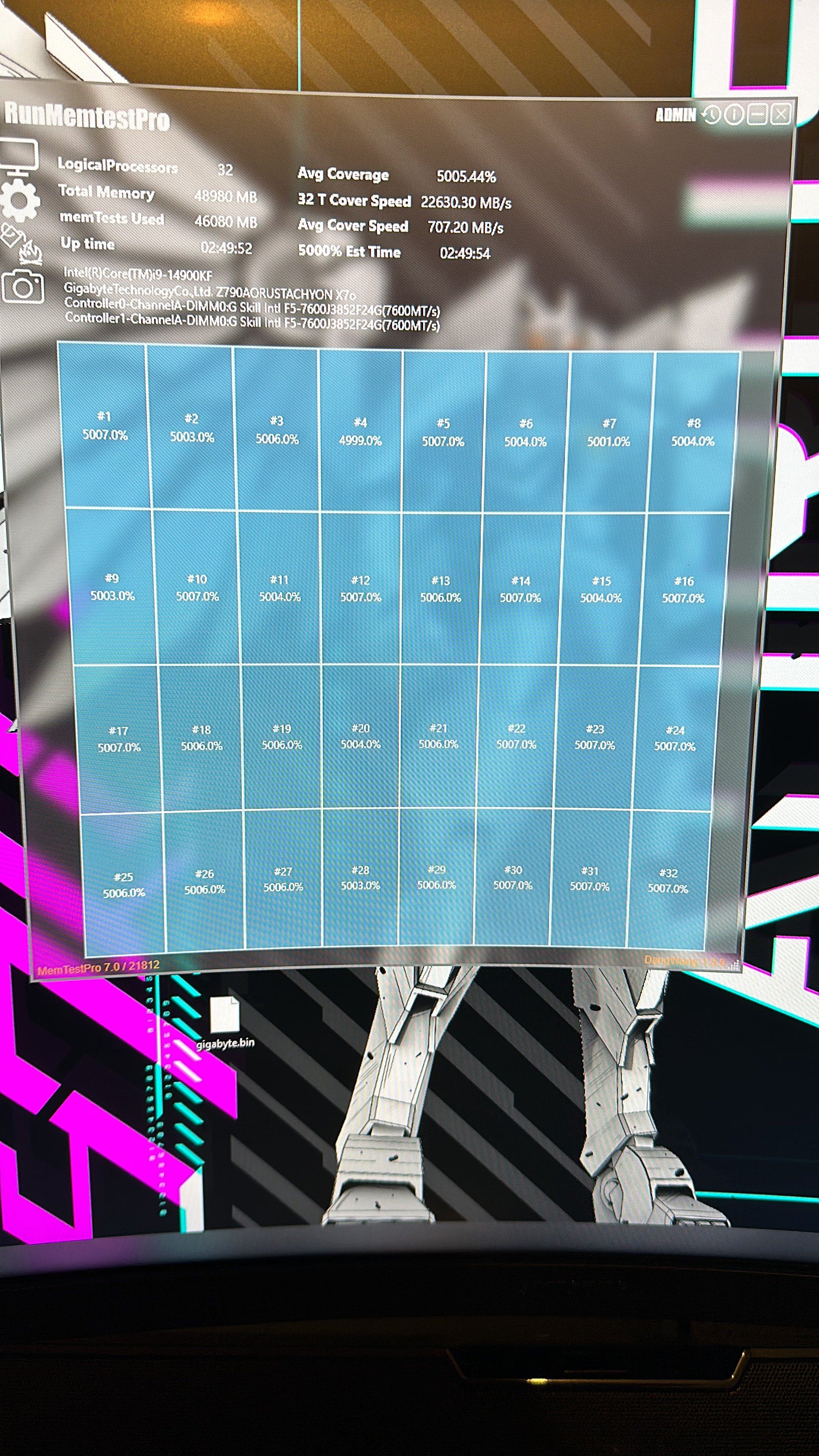


") unfortunate~
unfortunate~
")

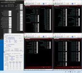
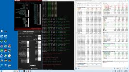
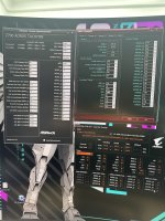
 .
.