Veii
Enthusiast
- Mitglied seit
- 31.05.2018
- Beiträge
- 1.480
- Desktop System
- QA Platform
- Laptop
- ASUS 13" ZenBook OLED [5600U]
- Details zu meinem Desktop
- Prozessor
- Intel Core Ultra 9 285K
- Mainboard
- ASRock OC Formula
- Kühler
- Alphacool T38 280mm
- Speicher
- G.Skill Z5 CK 9600
- Grafikprozessor
- GTX1080ti KP [XOC ROM] // EVGA GTX 650 1GB [UEFI GOP]
- Display
- KOORUI GN10 miniLED
- SSD
- Samsung EVO 850
- Soundkarte
- ESI Ambier i1 & AKG P820
- Gehäuse
- Open-Bench
- Netzteil
- Corsair SF85 // Seasonic GX-550
- Keyboard
- Topre Realforce 108UBK 30g [Silenced]
- Mouse
- Endgame-Gear OP1 8K
- Betriebssystem
- Win11
- Internet
- ▼42 MBit ▲15 MBit
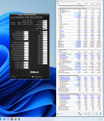
@zebra_hunNiedrige VDDQ_CPU hat #0 dropouts.
Ebenso RTT issues, VREF issues.
2 (PARK) & 10 (NOM) ~ RTT = DQ issues.
Beitrag automatisch zusammengeführt:
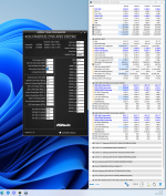
Nee mit dem neuen Bios können wir vieles nicht nutzen.7200 und 7600 mit odt's. Leider Werte, die da passen, beim 8000 gehts nicht. Es ist auto jetzt.
Ohne odt's 7200 geht auch nicht.
Odt's von dir, ca zwei Monate früher, nur bischen sollte ich durharbeiten. Von kopf weiss ich nicht, ich muss das Profil einladen.
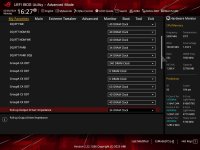
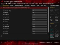
ODT ok vlt
Aber eher weniger.
RTT eher nein.
2 & 10 sind RTT Probleme.
RONs könnten noch passen.
Der Rest ist fragwürdig.
Zuu viele Änderungen mittels ASUS's Seite.
")


")