Du verwendest einen veralteten Browser. Es ist möglich, dass diese oder andere Websites nicht korrekt angezeigt werden. Du solltest ein Upgrade durchführen oder einen alternativen Browser verwenden.
Nicht schwer zu verstehen eigentlich, eintragen und auslesen ist etwas anderes als das was der Controller bzw. die Intel CPU tatsächlich macht mit den Werten.
Die tRTP ist ebenfalls ein schlechtes Beispiel. da kann man auch eintragen was man möchte der valide Wert ist für jede Intel CPU bei DDR5 in Sachen Precharge die tRDPRE.
Daher kannst du ja auch überall 4 oder 0 bei DR und DD Eintragen diese Werte verwirft der Controller einfach bei DIMMs die eben keine verschiedenen Ränge haben, sprich das wird ebenfalls zu keinem Fehlern in Testmem5 führen basierend auf dem Bild was gepostet wurde.
Natürlich sollte immer die 8 rein bei "TRDRD_dg" und "TWRWR_dg", die meisten Tertiary Timings wird die CPU aber vorher angepasst haben sollten sie zu stark aus der Reihe tanzen.
Wenn nicht wird man sich evtl. sogar die performance halbiert haben wie xl_digit beispielsweise ohne es zu merken,
Datenschutzhinweis für Youtube
An dieser Stelle möchten wir Ihnen ein Youtube-Video zeigen. Ihre Daten zu schützen, liegt uns aber am Herzen: Youtube setzt durch das Einbinden und Abspielen Cookies auf ihrem Rechner, mit welchen sie eventuell getracked werden können. Wenn Sie dies zulassen möchten, klicken Sie einfach auf den Play-Button. Das Video wird anschließend geladen und danach abgespielt.
Youtube Videos ab jetzt direkt anzeigen
.
Aber wer natürlich auf 7,9,11,13 und sechstellige tREFI usw. steht ohne zu wissen was die Timings überhaupt machen kann die natürlich eintragen .
Die ausgelesenen Werte sind auch korrekt, ich glaub der ASRock Timing Configurator ließt den runtimewert aus in Windows, Memtweak die BIOS Werte. Es ist ein von der CPU vergebener Wert nach Formel der keine wirkliche Relevanz hat da darf man sich nicht irritieren lassen was ausgelesen wird.
Hab's mal bestellt 😉
Woher hast du das 8600Mhz Ergebnis?
OK, habs gefunden:
Datenschutzhinweis für Youtube
An dieser Stelle möchten wir Ihnen ein Youtube-Video zeigen. Ihre Daten zu schützen, liegt uns aber am Herzen: Youtube setzt durch das Einbinden und Abspielen Cookies auf ihrem Rechner, mit welchen sie eventuell getracked werden können. Wenn Sie dies zulassen möchten, klicken Sie einfach auf den Play-Button. Das Video wird anschließend geladen und danach abgespielt.
Yes, the intuition is good. I see that the problem is not to be found in the RAM OC.
I would show you a very ugly picture again.
This is the Default BIOS with the 14900k, 8C water cooling.
100C in ~ 5 seconds under Cinebench.It's not a big load, but this horrible cpu is 100C immediately even with such cooling. I'm not the only one, all my fellow forum members here in Hungary can buy one. It's all like that.
Now I realized, I understood why I actually don't have a problem even with 8000MHz OC profiles.
This VT3 is not a RAM test, it's a CPU test.
It requires a very high Vcore, which is unnecessary in real life.
HCI, TM5, etc. it passes, it also passes VT3 with a high Vcore.
VT3=CPU test in my eyes.
Throttled to 5200-5300MHz, but in BIOS 54xP 40xE Ring=auto (45x)
I entered a limit of 85C and a 250/270W + 400A.
At the moment, everything is as you described, the entire voltage control is automatic.
I know this PC well, I know, I feel that it can run for hours in this form, but I stopped it, sorry.
The whole 13-14. generation is a horror in my eyes, they work fine on low load, but on a strong load, the described many MHz is a lie.
It just hurts to watch throttling.
All my life I set the Vcore by choosing a well-cooling frequency, looking for the CbR23 Vmin, adding ~20mV to it.
Later i will to search a Vmin for Y VT3, maybe...
With auto Voltages a Cinebench can't run without trottling.
I think, memory oc isn't bad.
Yes, the intuition is good. I see that the problem is not to be found in the RAM OC.
I would show you a very ugly picture again.
This is the Default BIOS with the 14900k, 8C water cooling.
100C in ~ 5 seconds under Cinebench.It's not a big load, but this horrible cpu is 100C immediately even with such cooling. I'm not the only one, all my fellow forum members here in Hungary can buy one. It's all like that.
Now I realized, I understood why I actually don't have a problem even with 8000MHz OC profiles.
This VT3 is not a RAM test, it's a CPU test.
It requires a very high Vcore, which is unnecessary in real life.
HCI, TM5, etc. it passes, it also passes VT3 with a high Vcore.
VT3=CPU test in my eyes.
Throttled to 5200-5300MHz, but in BIOS 54xP 40xE Ring=auto (45x)
I entered a limit of 85C and a 250/270W + 400A.
At the moment, everything is as you described, the entire voltage control is automatic. Anhang anzeigen 952731
I know this PC well, I know, I feel that it can run for hours in this form, but I stopped it, sorry.
The whole 13-14. generation is a horror in my eyes, they work fine on low load, but on a strong load, the described many MHz is a lie.
It just hurts to watch throttling.
All my life I set the Vcore by choosing a well-cooling frequency, looking for the CbR23 Vmin, adding ~20mV to it.
Later i will to search a Vmin for Y VT3, maybe...
With auto Voltages a Cinebench can't run without trottling.
I think, memory oc isn't bad.
I understand the frustration
And i am completely agreeing with Steve from GN for this generation + some ASUS-HQ members.
But its what is fused and thats what you get.
ASUS tries a lot already, although on stock those Boards come with unlocked limiters.
Soo who would you judge here.
The thing you may not know is, that it targets 105° per core.
The Throttling Algo is changed (supported on 13900KS) with a 10° higher Thermal Ceiling and +200MHz more.
Its a different color substrate with own little properties changes. 105° is perfectly OK.
Its not a 1:1 rebrand. Well~
Its not bad solder either, its completely intentional for some cores to be 7° lower while others reach 105°.
What is not such a nice story, is the overvoltage of those samples from the factory on & that current XTREEM Powerprofile is not well tuned for short and long power-loads.
The transient peaks are alright. Its bad, but its equally bad like last gen.
Please ! don't take away voltage this way.
You mess with the CPU.
Do it with the V/F points and do it with the IA Loadline.
This is the correct way.
Because the curve is not completely unison, it is important to add some voltage back on the V/F curve.
It is a very very bad idea to cut voltage from the send.
Let it deliver what it has to deliver, but spoof the telemetry. Don't spoof the supply. This causes a runaway scenario.
Also do not fix clock please. Do that with amperage limiters and voltage limiters. Leave the CPU be the CPU it was designed with.
Just adjust the telemetry a bit lower, as margins left are high;
Now I realized, I understood why I actually don't have a problem even with 8000MHz OC profiles.
This VT3 is not a RAM test, it's a CPU test.
It requires a very high Vcore, which is unnecessary in real life.
HCI, TM5, etc. it passes, it also passes VT3 with a high Vcore.
VT3=CPU test in my eyes.
All my life I set the Vcore by choosing a well-cooling frequency, looking for the CbR23 Vmin, adding ~20mV to it.
Later i will to search a Vmin for Y VT3, maybe...
I can try to explain if you are open minded.
But its not that easy.
Cinebench is using AVX2/512 instructions
Y-Cruncher VST is using an Iteration of AVX2
But VT3 is a mixed load. Its purpose is to fill the bufferqueue and completely max out cache, ring and show irregularities when data moves towards mem, as cache is full.
It is targeted to be as rough as possible *, so is N63 (early N64) now.
VT3 is a new Iteration of a "blend FFT" test, just purposely rough
// * because usually L$ of CPUs is big and fast. Plus accelerators are intelligent and cut complex instructionsets to small bits = lower heat.
// It's hard to actually max out a CPU and then test real performance limits. "We" are mostly fooled by our little benchmarks that barely max out whatever you throw at it,. Neither mem nor cache.
// Nor are games even remotely close to maxing out CPU or Mem. They are usually not well designed vs our analytical stuff & that bad design has a higher chance to leak to mem (if the texture is huge), but still. The point stays;
An SSE load which may be games if badly coded
Are high vcore.
Vcore is not everything and amperage at the end is what makes it
The lower the CPU has to throttle vcore, the harsher the load actually is ~ or the less of instructions it actually manages to fullfill, hence lower voltage is needed
That here it (cores and especially ring) starves for voltage
Is a side-issue and why this test is soo much harder on Intel vs on AMD.
High voltage Load is the most weakest load.
Here it jumps fast. You the user don't really notice voltage shifting by those slowly reporting tools.
You need to track it within 10ms,, to actually see what's going on.
Don't be scare or fooled by the voltage.
The heat is ok. Its evil , it really is
But its necessary.
You can AVX offset that later on, but you purposely want to hold stability at a throttle state
Throttling is not a bad thing since 3-4 years.
But that's another huge topic to explain.
Set normal clock (MHz) already doesn't mean real clock
Because everything is loadbalanced and usable IOPS don't have to match target clock.
Y-cruncher now gives you a calculation speed value, which you can try to track throttling with.
One that happens at same clock-strap ~ but with CEP disabled, you prevent one of the steps (well 2) of internal throttle. Soo it will rather crash with it disabled. Thats ok~~
Beitrag automatisch zusammengeführt:
@zebra_hun one last thing
You should also keep in mind that voltage supply to vcore and e-cores + ring
Is also load balanced. LDO's
Memory Controller voltage is not VDDIO/MC_Voltage
MemController takes a chunk of vcore too.
Voltages are intertwined and the OC/XOCer has no permission to change that.
VDDCR_IA voltage is taken away.
VDDCR_SA is given ~ but even that voltage changes scaling of other voltages and influences ODT of the CPU
ODT of the CPU completely changes strength of whatever voltage it is.
Soo what is dangerous or not - is strongly situation based.
Voltage itself is not the issue. Voltage alone doesn't mean anything;
// For memory the same. Voltage means nothing, RTTs make and break it
Keep your limiters active . . .
Don't force clock or vcore if you care for your CPU
Shift them , so you don't disable the dynamicnes of it
It was a bit old, i corrected
Mid discussion with bianbao.
He is right, i was right but a bit blind
Personally its slightly higher than RFC. RFCpb is around 30ns lower than RFC (depends)
I dont want to recommend a formula, because "tRFC mini" existed to combat rounding mistakes
This was a problem since Zen2/3, and my docs had 2-3 years of maintenance put into it (still have stuff to fix)
Giving you the formula still will create rounding mistakes. Better use the public sheet and if i find motivation, i'll extend the DDR5 part a bit more.
DDR4 part was focused on a discharge algo, which needed time to get correct. Same time rounding errors issues appeared.
I think i've sorted that out and suggest you to just go and use that for tXSR or not bother with that timing.
Its nearly a half as low value as JEDEC predicted is.
Don't think ASUS-HQ has that part already implemented.
Many of the older stuff is but no credits, ah i dont mind.
Hope more Boardpartners follow and fix bioses.
I'm not JEDEC sheet writer either, nor Micron™ to give specs till 8800MT/s ~ soo i dont deserve credit
Still~
DFE on Receiver side is under question, can be on , unlikely to bother, but under question
FGR aways on
RTL Training i would not enable it for Asus boards. Generally would never
RTL R2-R7 off, well R4-R7 up to channel used ~ can be. Links are build, Off can be good if possible.
Same for _DR on Single Sided, timings are added ontop. Want it or not. It often is just a waste to do so ,, soo if possible zero them out.
Pull UP-Downs are written on the last OCN post
Either go full manual, or don't touch them
Bad values there will cause per channel issues.
Given ASUS Boards get little complains on that (haha, they do well now tho)
i would not touch.
Per channel issues depend on memory controller too,
Soo there is your target.
You can try to go full manual mode like i did,, but its pain
Bootable max is higher, because you earned it by work - but its still pain
I don't recommend~~
But i dont deny either. RONs are just for far far down the line. Before that Groups have to be ok
Before that, you need to know value scaling for chip+board. Then you can touch RTT and Groups (and need to offset your target value with same learned scaling delta)
I don't think thats a leaky chip at all.
Resources for 13th gen are little
But this looks quite the opposite of leaky.
Go with low voltage and low SA. Anhang anzeigen 952670
Leave R1 on.
Leave RON training on Auto
Disable RTL Training. Board has a lookup table.
VDDQ Training only if you bench and look for max clock.
Off if you like torture but want to spend the time finding correct VDDQ delta to mem VDDQ.
Leave _DD timings alone
And Auto WRPRE + WRPDEN , use WTR & WR manually as your input. Let board do the math
XP, CKE, CPDED, XSDLL you always want to scale by clock
XSR is a bonus, but you need to scale RFC else you get issues
For higher OC either enabling TVB or putting V/F 11 on + 0.010 to 0.015 is a good idea
Instead of using global vcore offset
Core and Ring PLL idk if you would need. You influence voltage supply that way. But you know your cpu
Anhang anzeigen 952672
Always manual, do not trust the board.
Same for SA ~ try 1.18 for now, then try 1.22 if nothing helps Anhang anzeigen 952673
^ Please dont do that tho.
Removing vcore just to increase PLL, is silly
You mess with the cpu voltage recognition circuit.
MRC Fast Boot
& Fastboot
Both OFF
On, only for XOC or EZ mode
1. About tXSR, i have read that tRFCpb=tRFC/1.23, so if i use tRFC 512, tRFCpb should be 416. How much should tXSR be? Sorry i ask again but i want to have that clear in mind I can ofc leave that on Auto, but i have seen you recommended a fixed value on previous posts.
2. I thought enabling RTL tighten RTLs and give better performance, its not true?
3. With VDDQ training off i managed to get VT3 10 loops stable, (i am not willing to run for more, after all thats only a gaming pc) with VDDQ_CPU 1.24v - VDDQ_DIMM 1.47v. So the auto at 1.35v was very far off. Also i read in OCnet that 0801 need less volt that the previous bios but i didnt expect such a big difference. With 0701 i needed 1.38v for 8000C36.
4. About _DD timings, i had set them at 0 because on a previous post, you said so
5. Everyone set WTR_L/S through WRRD_sg/dg. Is that wrong? What are the optimal values if i have to set the directly for 8000-8200C36?
6. WRPRE(/WRPDEN) set WR, correct? Why on auto then?
7. Core PLL is said to help with Core Vmin and is useful. You think its better on Auto even if i need more vcore?
8. Now that i got VT3 stable i can turn MRC Fast Boot/Fast Boot at Enabled or i keep them always OFF?
9. MCH Full Check on/off?
I attach both VT3 screenshot and .txt, if you see anything abnormal let me know.
If i can go any tighter at 8000C36 tell me what to change and i ll give it a shot. if thats the max i can get from 8000 then lets go to 8200
Shenanigans. Miracles
Fairy Tales ~ call it how you want
The only person that knows the board the best, is not the attempts of training
But the Boardpartner who designed the Board and the Bios of it.
ASUS has correct RTLs.
Its perfect with it and strives for perfection (as that limits max clock)
Soo its kinda first priority to get this flawless when you want your Board to be in the Leaderboards.
Just out of logic on things that are already done 🤭
If ASUS is great at something, that is Bios tuning.
If they want to implement every tuning, at lower SKUs is another question tho~~
3. With VDDQ training off i managed to get VT3 10 loops stable, (i am not willing to run for more, after all thats only a gaming pc) with VDDQ_CPU 1.24v - VDDQ_DIMM 1.47v. So the auto at 1.35v was very far off. Also i read in OCnet that 0801 need less volt that the previous bios but i didnt expect such a big difference. With 0701 i needed 1.38v for 8000C36.
Delta is first Board PCB quality and then CPU Leakage ability ~ dependent
Then you add Dimm-PCB quality and thats about the value you get up with.
Its very important (i feel) to test that long and learn it. Every sample is unique.
VDDQ builds VREF and VREF is basically your main target.
If DQS is bad, forget high clock or anything higher than 6400MT/s. Even that can be hard but should be "ok" with Gear2.
Specs only cover till 6400MT/s, early till 5600MT/s.
Some CPUs then have more some less margins left.
Hence some users can be more some need to be less lazy and get everything perfect.
You may have forgotten that you need to run VST+VT3.
Running only one will have a different effect and not showcase an error, if there is one.
I don't run the same perfectionistic value as my early Team (6 hours of y-cruncher VST+VT3)
But at least 90min is a requirement. 45-90min up to roomsize.
There is no argumentation point for laws of physics This goes for testing GPUs, Memory or CPUs. 90min minimum, sorry.
I dont know what to comment on the other half of the comment
_DR timings to zero
DD are loaded. Both are loaded, but _DR has no need to exist. Just a waste of delay.
_DR to zero for single sided dimms.
If _DR are at Zero (not Auto, not 1) then R2-R7 or R4-R7 (1DPC or 2DPC) need to be at value zero.
My methods are unconventional and pragmatic (lazy).
It is correct to set it with WRRD, but this increases the chance of user blindness.
You always need to do the math on a formula which i see is incorrect due to dimm utillization method.
ASUS has the Formula correct ~ on Gigabyte i saw calculation issues.
Set WTR and WR manually, leave the Board up to FW state adapt its formula's
ODMs & FW-Team's work is to get those values correct. It should not be users work
Same reason above
But WRPDEN is wrong so far for all of them. ASUS-HQ got their stuff together now.
I dont trust auto anything, but same reason above. Will cause trouble with clock shifting and is unnecessary much work.
Just set tWR and don't deal with them.
If its calculated wrong, we will notice.
Nobody should resort to PLLs.
This is also Boardpartners work to get their boards and Firmware together.
Auto = predicted up to Bios.
Keep it that way
Its not common that Bioses, especially ASUS ones tell you what they actually load.
Unfortunately that's reality. Soo you may have made things worse by fixing a voltage you don't know its current state.
Using PLLs if there are bios bugs, may also permanently mess with your CPU till hardreset.
Hardreset = outside for days till everything internal loses charge and forgets persistent settings.
On this actually Buildzoid and Co did notice that MemController remembers nonsense till CPU was pulled out of the socket.
It shouldn't cause anymore such bugs (one of those was perma 00h on boot)
And too high PLLs will cause that state till CMOS reset also resets it (not common early on)
Soo no touch there. You mask and go around the main issue. Its more work but please trust me here.
Going around an issue with a bandaid is the worst you can do ,with already that many variables
Always off.
But thats me.
Both off causes a longer training.
There are 11+ lets call them Rails, ,between the CPU and each memory stick ~ which need to nearly perfectly align before timings start to matter.
Training is required and long training even more.
Its not as bad as 90-120sec training on AMD.
Intel users have that luxury, soo i would keep it off
Because those 5sec less can hardbreak stability
You as user still don't have access to 30 more timing options that are trained in the background.
Keep it off, training is important .
Only enable it if you want to push and dont trust the board to retrain correctly on a trained-lowerclock state.
I personally like accuracy over believe. Soo with lack of believe i prefer control , which means no random short-training variables please.
Sadly unsure.
It never worked for me early on.
A lot has changed last 3 months on the FW Team of ASUS.
Soo it may be functional - but i dont know.
This type of full training will help
But then , it making a difference only shows that something was bad to begin with
Training is either correct or half complete, or just bad.
Short training will not change this variable much, as long as it actually does train and not just bruteforce presets.
Auto is a good value here.
1. About tXSR, i have read that tRFCpb=tRFC/1.23, so if i use tRFC 512, tRFCpb should be 416. How much should tXSR be? Sorry i ask again but i want to have that clear in mind I can ofc leave that on Auto, but i have seen you recommended a fixed value on previous posts.
RFCpb under personal active research.
There is no spec for this.
Because we dont follow spec.
For 16gb dimms its around 110-115ns in OC'd state.
When RFC is 140-150ns (dont mind that one doesnt target 120ns)
I always target silly stability targets.
Never had good cooling Im a researcher, not an XOCer.
RFC you want to stay in steps of 32.
REFi you want to stay in steps of 8192 (endvalue -1 , for bios input)
Soo target RFC for 8000MT/s is around
544.
Expected stability near 1.4 VDD
would be RFCpb 448 or 480.
You will see TM5 crash with something like this
If RFCpb is too low. Not my picture~
RFCpb just needs to be lower than RFC.
For 544 RFC = 583 XSR
20 CKE & CPDED, 30 tXP
Keep in mind, my XSR is very tight. Be sure to isolate it as own error-variable.
Unsure how boardpartners calculate that, likely from JEDEC RFC.
But their value is in the 1000 range & doesnt care about user-input RFC. I don't agree with that way of tuning-comfort. Its a scaling value.
This will improve perf but requires remain powerdown timings to be flawless too.
Which they are still not for many of the Biosrevisions i've seen. Many Boardpartners i mean;
8200MT/s
CPU System Agent Voltage Override [1.21000] → no touch, else VDDQ re'check.
^ Potentially drop to 1180 much later on.

Memory Controller Voltage [1.41250] → 1.43
DRAM VDD Voltage [1.51000] → 1.53

IVR Transmitter VDDQ Voltage [1.24000] → no touch
DRAM VDDQ Voltage [1.48000] → no touch
This is how you scale
SA is standalone and messes with scaling of other 2 packages, messes with ODT after X range.
Other two packages scale together. Starting value of both are influenced by Bios predicted ODT (Groups), RON & RTTs.
Of course TermPLL changes the whole thing ~ soo no touch on PLL for now.
VDD is kind of standalone
VDDQ is together. Shift one shift the other. After you know your delta;
~ where 10min y-cruncher is nothing. Needs 90min and both tests.
I think no need to add voltage here. Its already plenty.
Primaries look realistic for 8200.
Else +2 CAS, +1 RCD. So far no need.
EDIT ~ Potentially RFCpb to 480 too, for 8200MT/s. Its very tight predicted.
EDIT:
Thinking more about it
Your CPU was low leakage
You might even be able to run 8000MTs @ 1.12 SA // 1.22 VDDQ_CPU, 1.46 VDDQ_MEM // 1.36 VDD2_CPU, 1.5 VDD_MEM
I think it could pass~
Near 1.12-1.14 i see SA for you. and around 1.32-1.35 VDD2_CPU.
But then again, all values go in pairs soo my imaginary preset is higher.
// Those values will be higher for other leakier CPUs on other Mainboards with other Bios revisions;
And also your test wasn't really confirming stability ~ sorry, its just too short for me to say "ok".
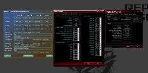
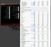
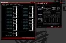
Hello @all, again I tried reading alot but still not understanding all like DDR4 where I was an OC Monster. These are my Results for now. Any Tipps to make it maybe better/ tighter?
@Veii Before i go on with testing, this is how you like the timings?
In bios
WRRD_sg/dg-WRPRE-WRPDEN Auto
tWR 24
tWTR_L/S 22/4 In windows show as 28/10 in Asrock, 24/6 in Hwinfo
Okay. Before I resettet my BIOS 6800mhz was easy booting but on Aida it made Hardware Erros. Today I resettet all. Tweaked my CPU again like 1.296 Vcore 5,3GHZ All core. After stable loaded XMP I not II or Tweaked like I did before. Than Tweaked some Timings and than used Maximus Tweak Mode 2.
Like you said now I did Auto on R3 RTL MCH. I lowered SA pending 1.232 to 1.248. I Set in Bios TWR 62 but in Mem Tweak it shows 65
Do I need to give more Voltage somewhere for 6800 MHZ or just click and boot an test? How low more i can go TWR? What is with tRAS, tWCL,tRTP
My latency is pending between 59,5 and 60,7 atm.
Anyways other more Ideas or Tightening trys/ options? What about the classic TRFC lowering? But higher Trefi is firstly better than lower trfc?
I did not any further tests now just played some games and did 5 mins of Prime 95 Blend
@Veii Before i go on with testing, this is how you like the timings?
In bios
WRRD_sg/dg-WRPRE-WRPDEN Auto
tWR 24
tWTR_L/S 22/4 In windows show as 28/10 in Asrock, 24/6 in HwinfoAnhang anzeigen 952856
Wow, almost made it.
I'll be able to handle this, it's finally responding the way it should.
I'll describe what caused the problem, although it shouldn't cause such a problem.
You wrote to reset the voltage to default. I saw that, it was finally working normally.
AC DC LL if not auto, immediately error. Now I made undervolt with V/F Curve.
I'm too old, i want UV to do. I'm not changing anymore, I'm old, lol.
I wanted to do a 90-minute Y for you, but it went wrong at the 80th minute.
But i'm happy, works fine
A BIG THX FOR YOU.
Ps.:
You gave me a lot of information, I will process it and use it. Not today, I will be with my children, I wish you good health and all the best!
Thank you
Mind you, the bare minimum
Team expects 6 hours, not 1.5hours
I would be ok with 4 hours too, but rather test PSU off - discharge, PSU on , stability test again.
ColdBoot Training variance is more important than a single run
But yes, Signal-Noise issues~
I expect then 20 000% Karhu too (if you use that tool)
Next to completed 25 cycles TM5 1usmus_V3
Finally there is a change when I change the voltages.
Now the dance begins.
DRAM VDD Voltage [1.47000]
DRAM VDDQ Voltage [1.44000]
IVR Transmitter VDDQ Voltage [1.30500]
Memory Controller Voltage [1.36250]
Next time i will try 1.31V VDDQ Tx after discharge PSU. If u have got better idea, tell me pls.
Here is the new BIOS:
[2023/12/27 21:21:43]
Ai Overclock Tuner [Auto]
Intel(R) Adaptive Boost Technology [Auto]
ASUS MultiCore Enhancement [Auto – Lets BIOS Optimize]
SVID Behavior [Auto]
BCLK Frequency : DRAM Frequency Ratio [100:100]
Memory Controller : DRAM Frequency Ratio [1:2]
DRAM Frequency [DDR5-7600MHz]
Performance Core Ratio [By Core Usage]
1-Core Ratio Limit [54]
2-Core Ratio Limit [54]
3-Core Ratio Limit [54]
4-Core Ratio Limit [54]
5-Core Ratio Limit [54]
6-Core Ratio Limit [54]
7-Core Ratio Limit [54]
8-Core Ratio Limit [54]
Performance Core0 Specific Ratio Limit [Auto]
Performance Core0 specific Voltage [Auto]
Performance Core1 Specific Ratio Limit [Auto]
Performance Core1 specific Voltage [Auto]
*Performance Core2 Specific Ratio Limit [Auto]
Performance Core2 specific Voltage [Auto]
*Performance Core3 Specific Ratio Limit [Auto]
Performance Core3 specific Voltage [Auto]
Performance Core4 Specific Ratio Limit [Auto]
Performance Core4 specific Voltage [Auto]
Performance Core5 Specific Ratio Limit [Auto]
Performance Core5 specific Voltage [Auto]
Performance Core6 Specific Ratio Limit [Auto]
Performance Core6 specific Voltage [Auto]
Performance Core7 Specific Ratio Limit [Auto]
Performance Core7 specific Voltage [Auto]
Efficient Core Ratio [By Core Usage]
Efficient Turbo Ratio Limit 1 [40]
Efficient Turbo Ratio Cores 1 [Auto]
Efficient Core Group0 Specific Ratio Limit [45]
Efficient Core Group0 specific Voltage [Auto]
Efficient Core Group1 Specific Ratio Limit [45]
Efficient Core Group1 specific Voltage [Auto]
Efficient Core Group2 Specific Ratio Limit [45]
Efficient Core Group2 specific Voltage [Auto]
Efficient Core Group3 Specific Ratio Limit [45]
Efficient Core Group3 specific Voltage [Auto]
AVX2 [Enabled]
AVX2 Ratio Offset to per-core Ratio Limit [User Specify]
AVX2 Ratio Offset [0]
AVX2 Voltage Guardband Scale Factor [User Specify]
AVX2 Voltage Guardband Scale Factor [0]
Maximus Tweak [Mode 2]
DRAM CAS# Latency [34]
DRAM RAS# to CAS# Delay Read [44]
DRAM RAS# to CAS# Delay Write [44]
DRAM RAS# PRE Time [44]
DRAM RAS# ACT Time [56]
DRAM Command Rate [2N]
DRAM RAS# to RAS# Delay L [12]
DRAM RAS# to RAS# Delay S [8]
DRAM REF Cycle Time 2 [480]
DRAM REF Cycle Time Same Bank [Auto]
DRAM Refresh Interval [131071]
DRAM WRITE Recovery Time [Auto]
DRAM READ to PRE Time [12]
DRAM FOUR ACT WIN Time [32]
DRAM WRITE to READ Delay L [24]
DRAM WRITE to READ Delay S [8]
DRAM CKE Minimum Pulse Width [19]
DRAM Write Latency [32]
Ctl0 dqvrefup [162]
Ctl0 dqvrefdn [80]
Ctl0 dqodtvrefup [Auto]
Ctl0 dqodtvrefdn [Auto]
Ctl1 cmdvrefup [Auto]
Ctl1 ctlvrefup [Auto]
Ctl1 clkvrefup [Auto]
Ctl1 ckecsvrefup [Auto]
Ctl2 cmdvrefdn [Auto]
Ctl2 ctlvrefdn [Auto]
Ctl2 clkvrefdn [Auto]
Read Equalization RxEq Start Sign [-]
Read Equalization RxEq Start [Auto]
Read Equalization RxEq Stop Sign [-]
Read Equalization RxEq Stop [Auto]
ODT_READ_DURATION [Auto]
ODT_READ_DELAY [Auto]
ODT_WRITE_DURATION [Auto]
ODT_WRITE_DELAY [Auto]
DQ RTT WR [40 DRAM Clock]
DQ RTT NOM RD [40 DRAM Clock]
DQ RTT NOM WR [40 DRAM Clock]
DQ RTT PARK [34 DRAM Clock]
DQ RTT PARK DQS [34 DRAM Clock]
GroupA CA ODT [240 DRAM Clock]
GroupA CS ODT [0 DRAM Clock]
GroupA CK ODT [0 DRAM Clock]
GroupB CA ODT [60 DRAM Clock]
GroupB CS ODT [40 DRAM Clock]
GroupB CK ODT [40 DRAM Clock]
Pull-up Output Driver Impedance [34 DRAM Clock]
Pull-Down Output Driver Impedance [34 DRAM Clock]
Round Trip Latency Init Value MC0 CHA [Auto]
Round Trip Latency Max Value MC0 CHA [Auto]
Round Trip Latency Offset Value Mode Sign MC0 CHA [-]
Round Trip Latency Offset Value MC0 CHA [Auto]
Round Trip Latency Init Value MC0 CHB [Auto]
Round Trip Latency Max Value MC0 CHB [Auto]
Round Trip Latency Offset Value Mode Sign MC0 CHB [-]
Round Trip Latency Offset Value MC0 CHB [Auto]
Round Trip Latency Init Value MC1 CHA [Auto]
Round Trip Latency Max Value MC1 CHA [Auto]
Round Trip Latency Offset Value Mode Sign MC1 CHA [-]
Round Trip Latency Offset Value MC1 CHA [Auto]
Round Trip Latency Init Value MC1 CHB [Auto]
Round Trip Latency Max Value MC1 CHB [Auto]
Round Trip Latency Offset Value Mode Sign MC1 CHB [-]
Round Trip Latency Offset Value MC1 CHB [Auto]
Round Trip Latency MC0 CHA R0 [Auto]
Round Trip Latency MC0 CHA R1 [Auto]
Round Trip Latency MC0 CHA R2 [0]
Round Trip Latency MC0 CHA R3 [0]
Round Trip Latency MC0 CHA R4 [0]
Round Trip Latency MC0 CHA R5 [0]
Round Trip Latency MC0 CHA R6 [0]
Round Trip Latency MC0 CHA R7 [0]
Round Trip Latency MC0 CHB R0 [Auto]
Round Trip Latency MC0 CHB R1 [Auto]
Round Trip Latency MC0 CHB R2 [0]
Round Trip Latency MC0 CHB R3 [0]
Round Trip Latency MC0 CHB R4 [0]
Round Trip Latency MC0 CHB R5 [0]
Round Trip Latency MC0 CHB R6 [0]
Round Trip Latency MC0 CHB R7 [0]
Round Trip Latency MC1 CHA R0 [Auto]
Round Trip Latency MC1 CHA R1 [Auto]
Round Trip Latency MC1 CHA R2 [0]
Round Trip Latency MC1 CHA R3 [0]
Round Trip Latency MC1 CHA R4 [0]
Round Trip Latency MC1 CHA R5 [0]
Round Trip Latency MC1 CHA R6 [0]
Round Trip Latency MC1 CHA R7 [0]
Round Trip Latency MC1 CHB R0 [Auto]
Round Trip Latency MC1 CHB R1 [Auto]
Round Trip Latency MC1 CHB R2 [0]
Round Trip Latency MC1 CHB R3 [0]
Round Trip Latency MC1 CHB R4 [0]
Round Trip Latency MC1 CHB R5 [0]
Round Trip Latency MC1 CHB R6 [0]
Round Trip Latency MC1 CHB R7 [0]
Early Command Training [Auto]
SenseAmp Offset Training [Auto]
Early ReadMPR Timing Centering 2D [Auto]
Read MPR Training [Auto]
Receive Enable Training [Auto]
Jedec Write Leveling [Auto]
Early Write Time Centering 2D [Auto]
Early Read Time Centering 2D [Auto]
Write Timing Centering 1D [Auto]
Write Voltage Centering 1D [Auto]
Read Timing Centering 1D [Auto]
Read Timing Centering with JR [Auto]
Dimm ODT Training* [Disabled]
Max RTT_WR [ODT Off]
DIMM RON Training* [Disabled]
Write Drive Strength/Equalization 2D* [Auto]
Write Slew Rate Training* [Auto]
Read ODT Training* [Disabled]
Comp Optimization Training [Auto]
Read Equalization Training* [Auto]
Read Amplifier Training* [Auto]
Write Timing Centering 2D [Auto]
Read Timing Centering 2D [Auto]
Command Voltage Centering [Auto]
Early Command Voltage Centering [Auto]
Write Voltage Centering 2D [Auto]
Read Voltage Centering 2D [Auto]
Late Command Training [Auto]
Round Trip Latency [Auto]
Turn Around Timing Training [Auto]
CMD CTL CLK Slew Rate [Auto]
CMD/CTL DS & E 2D [Auto]
Read Voltage Centering 1D [Auto]
TxDqTCO Comp Training* [Auto]
ClkTCO Comp Training* [Auto]
TxDqsTCO Comp Training* [Auto]
VccDLL Bypass Training [Auto]
CMD/CTL Drive Strength Up/Dn 2D [Auto]
DIMM CA ODT Training [Auto]
PanicVttDnLp Training* [Auto]
Read Vref Decap Training* [Auto]
Vddq Training [Disabled]
Duty Cycle Correction Training [Auto]
Periodic DCC [Auto]
Rank Margin Tool Per Bit [Auto]
DIMM DFE Training [Auto]
EARLY DIMM DFE Training [Auto]
Tx Dqs Dcc Training [Auto]
DRAM DCA Training [Auto]
Write Driver Strength Training [Auto]
Rank Margin Tool [Auto]
Memory Test [Auto]
DIMM SPD Alias Test [Auto]
Receive Enable Centering 1D [Auto]
Retrain Margin Check [Auto]
Write Drive Strength Up/Dn independently [Auto]
LPDDR DqDqs Re-Training [Auto]
Margin Check Limit [Disabled]
tRDRD_sg_Training [Auto]
tRDRD_sg_Runtime [16]
tRDRD_dg_Training [Auto]
tRDRD_dg_Runtime [8]
tRDWR_sg [20]
tRDWR_dg [20]
tWRWR_sg [16]
tWRWR_dg [8]
tWRRD_sg [Auto]
tWRRD_dg [Auto]
tRDRD_dr [0]
tRDRD_dd [Auto]
tRDWR_dr [0]
tRDWR_dd [Auto]
tWRWR_dr [0]
tWRWR_dd [Auto]
tWRRD_dr [0]
tWRRD_dd [Auto]
tRPRE [Auto]
tWPRE [Auto]
tWPOST [Auto]
tWRPRE [64]
tPRPDEN [2]
tRDPDEN [43]
tWRPDEN [65]
tCPDED [19]
tREFIX9 [Auto]
Ref Interval [Auto]
tXPDLL [Auto]
tXP [29]
tPPD [2]
tCCD_L_tDLLK [Auto]
tZQCAL [Auto]
tZQCS [Auto]
OREF_RI [Auto]
Refresh Watermarks [High]
Refresh Hp Wm [Auto]
Refresh Panic Wm [Auto]
Refresh Abr Release [Auto]
tXSDLL [2559]
tZQOPER [Auto]
tMOD [Auto]
CounttREFIWhileRefEn [Auto]
HPRefOnMRS [Auto]
SRX Ref Debits [Auto]
RAISE BLK WAIT [Auto]
Ref Stagger En [Auto]
Ref Stagger Mode [Auto]
Disable Stolen Refresh [Auto]
En Ref Type Display [Auto]
Trefipulse Stagger Disable [Auto]
tRPab ext [Auto]
derating ext [Auto]
Allow 2cyc B2B LPDDR [Auto]
tCSH [Auto]
tCSL [Auto]
powerdown Enable [Auto]
idle length [Auto]
raise cke after exit latency [Auto]
powerdown latency [Auto]
powerdown length [Auto]
selfrefresh latency [Auto]
selfrefresh length [Auto]
ckevalid length [Auto]
ckevalid enable [Auto]
idle enable [Auto]
selfrefresh enable [Auto]
Address mirror [Auto]
no gear4 param divide [Auto]
x8 device [Auto]
no gear2 param divide [Auto]
ddr 1dpc split ranks on subch [Auto]
write0 enable [Auto]
MultiCycCmd [Auto]
WCKDiffLowInIdle [Auto]
PBR Disable [Auto]
PBR OOO Dis [Auto]
PBR Disable on hot [Auto]
PBR Exit on Idle Cnt [Auto]
tXSR [645]
Dec tCWL [Auto]
Add tCWL [Auto]
Add 1Qclk delay [Auto]
MRC Fast Boot [Disabled]
MCH Full Check [Enabled]
Mem Over Clock Fail Count [2]
Training Profile [Auto]
RxDfe [Auto]
Mrc Training Loop Count [2]
DRAM CLK Period [Auto]
Dll_bwsel [Auto]
Controller 0, Channel 0 Control [Enabled]
Controller 0, Channel 1 Control [Enabled]
Controller 1, Channel 0 Control [Enabled]
Controller 1, Channel 1 Control [Enabled]
MC_Vref0 [Auto]
MC_Vref1 [Auto]
MC_Vref2 [Auto]
Fine Granularity Refresh mode [Auto]
SDRAM Density Per Die [Auto]
SDRAM Banks Per Bank Group [Auto]
SDRAM Bank Groups [Auto]
Dynamic Memory Boost [Disabled]
Realtime Memory Frequency [Disabled]
SA GV [Disabled]
Voltage Monitor [Die Sense]
VRM Initialization Check [Enabled]
CPU Input Voltage Load-line Calibration [Auto]
CPU Load-line Calibration [Auto]
Synch ACDC Loadline with VRM Loadline [Disabled]
CPU Current Capability [Auto]
CPU Current Reporting [Auto]
Core Voltage Suspension [Auto]
CPU VRM Switching Frequency [Auto]
VRM Spread Spectrum [Auto]
CPU Power Duty Control [Auto]
CPU Power Phase Control [Auto]
CPU Power Thermal Control [125]
CPU Core/Cache Boot Voltage [Auto]
CPU Input Boot Voltage [Auto]
PLL Termination Boot Voltage [Auto]
CPU Standby Boot Voltage [Auto]
Memory Controller Boot Voltage [Auto]
CPU Core Auto Voltage Cap [Auto]
CPU Input Auto Voltage Cap [Auto]
Memory Controller Auto Voltage Cap [Auto]
Maximum CPU Core Temperature [85]
Fast Throttle Threshold [Auto]
Package Temperature Threshold [Auto]
Regulate Frequency by above Threshold [Auto]
IVR Transmitter VDDQ ICCMAX [Auto]
Unlimited ICCMAX [Auto]
CPU Core/Cache Current Limit Max. [400.00]
Long Duration Package Power Limit [265]
Package Power Time Window [Auto]
Short Duration Package Power Limit [280]
Dual Tau Boost [Disabled]
IA AC Load Line [Auto]
IA DC Load Line [Auto]
IA CEP Enable [Disabled]
SA CEP Enable [Disabled]
IA SoC Iccmax Reactive Protector [Auto]
Inverse Temperature Dependency Throttle [Auto]
IA VR Voltage Limit [1500]
CPU SVID Support [Auto]
Cache Dynamic OC Switcher [Disabled]
TVB Voltage Optimizations [Disabled]
Enhanced TVB [Disabled]
Overclocking TVB [Disabled]
Overclocking TVB Global Temperature Offset Sign [+]
Overclocking TVB Global Temperature Offset Value [Auto]
Offset Mode Sign 1 [+]
V/F Point 1 Offset [0.00100]
Offset Mode Sign 2 [+]
V/F Point 2 Offset [0.00100]
Offset Mode Sign 3 [+]
V/F Point 3 Offset [0.00100]
Offset Mode Sign 4 [+]
V/F Point 4 Offset [0.00100]
Offset Mode Sign 5 [-]
V/F Point 5 Offset [0.02000]
Offset Mode Sign 6 [-]
V/F Point 6 Offset [0.06000]
Offset Mode Sign 7 [-]
V/F Point 7 Offset [0.06000]
Offset Mode Sign 8 [-]
V/F Point 8 Offset [0.06000]
Offset Mode Sign 9 [-]
V/F Point 9 Offset [0.06000]
Offset Mode Sign 10 [-]
V/F Point 10 Offset [0.06000]
Offset Mode Sign 11 [-]
V/F Point 11 Offset [0.06000]
Initial BCLK Frequency [Auto]
Runtime BCLK OC [Auto]
BCLK Amplitude [Auto]
BCLK Slew Rate [Auto]
BCLK Spread Spectrum [Auto]
Initial PCIE Frequency [Auto]
PCIE/DMI Amplitude [Auto]
PCIE/DMI Slew Rate [Auto]
PCIE/DMI Spread Spectrum [Auto]
Cold Boot PCIE Frequency [Auto]
Realtime Memory Timing [Disabled]
SPD Write Disable [TRUE]
PVD Ratio Threshold [Auto]
SA PLL Frequency Override [Auto]
BCLK TSC HW Fixup [Enabled]
Core Ratio Extension Mode [Disabled]
FLL OC mode [Auto]
UnderVolt Protection [Disabled]
Switch Microcode [Current Microcode]
Xtreme Tweaking [Disabled]
Core PLL Voltage [Auto]
GT PLL Voltage [Auto]
Ring PLL Voltage [Auto]
System Agent PLL Voltage [Auto]
Memory Controller PLL Voltage [Auto]
Efficient-core PLL Voltage [Auto]
CPU 1.8V Small Rail [Auto]
PLL Termination Voltage [Auto]
CPU Standby Voltage [Auto]
PCH 1.05V Voltage [Auto]
PCH 0.82V Voltage [Auto]
CPU Input Voltage Reset Voltage [Auto]
Eventual CPU Input Voltage [Auto]
Eventual Memory Controller Voltage [Auto]
Package Temperature Threshold [Auto]
Regulate Frequency by above Threshold [Auto]
Cooler Efficiency Customize [Keep Training]
Cooler Re-evaluation Algorithm [Normal]
Optimism Scale [100]
Ring Down Bin [Auto]
Min. CPU Cache Ratio [Auto]
Max. CPU Cache Ratio [47]
BCLK Aware Adaptive Voltage [Auto]
Actual VRM Core Voltage [Auto]
Global Core SVID Voltage [Auto]
Cache SVID Voltage [Auto]
CPU L2 Voltage [Auto]
CPU System Agent Voltage [Manual Mode]
- CPU System Agent Voltage Override [1.12500]
CPU Input Voltage [Auto]
High DRAM Voltage Mode [Enabled]
DRAM VDD Voltage [1.47000]
DRAM VDDQ Voltage [1.44000]
IVR Transmitter VDDQ Voltage [1.30500]
Memory Controller Voltage [1.36250]
MC Voltage Calculation Voltage Base [Auto]
VDD Calculation Voltage Base [Auto]
PMIC Voltages [Auto]
PCI Express Native Power Management [Enabled]
Native ASPM [Disabled]
DMI Link ASPM Control [Disabled]
ASPM [Auto]
L1 Substates [Disabled]
DMI ASPM [Disabled]
DMI Gen3 ASPM [Disabled]
PEG - ASPM [Disabled]
PCI Express Clock Gating [Enabled]
Hardware Prefetcher [Enabled]
Adjacent Cache Line Prefetch [Enabled]
Intel (VMX) Virtualization Technology [Disabled]
Per P-Core Control [Disabled]
Per E-Core Control [Disabled]
Active Performance Cores [All]
Active Efficient Cores [All]
Hyper-Threading [Enabled]
Hyper-Threading of Core 0 [Enabled]
Hyper-Threading of Core 1 [Enabled]
Hyper-Threading of Core 2 [Enabled]
Hyper-Threading of Core 3 [Enabled]
Hyper-Threading of Core 4 [Enabled]
Hyper-Threading of Core 5 [Enabled]
Hyper-Threading of Core 6 [Enabled]
Hyper-Threading of Core 7 [Enabled]
Total Memory Encryption [Disabled]
Legacy Game Compatibility Mode [Disabled]
Boot performance mode [Auto]
Intel(R) SpeedStep(tm) [Enabled]
Intel(R) Speed Shift Technology [Disabled]
Turbo Mode [Enabled]
Acoustic Noise Mitigation [Disabled]
CPU C-states [Auto]
Thermal Monitor [Enabled]
Dual Tau Boost [Disabled]
VT-d [Disabled]
Memory Remap [Enabled]
Enable VMD controller [Enabled]
Map PCIE Storage under VMD [Disabled]
Map SATA Controller under VMD [Disabled]
M.2_1 Link Speed [Auto]
PCIEX16(G5)_1 Link Speed [Auto]
PCIEX16(G5)_2 Link Speed [Auto]
PCIEX1(G4) Link Speed [Auto]
PCIEX4(G4) Link Speed [Auto]
M.2_2 Link Speed [Auto]
DIMM.2_1 Link Speed [Auto]
DIMM.2_2 Link Speed [Auto]
SATA Controller(s) [Enabled]
Aggressive LPM Support [Disabled]
SMART Self Test [Enabled]
M.2_3 [Enabled]
M.2_3 Hot Plug [Disabled]
SATA6G_1 [Enabled]
SATA6G_1 Hot Plug [Disabled]
SATA6G_2 [Enabled]
SATA6G_2 Hot Plug [Disabled]
SATA6G_3 [Enabled]
SATA6G_3 Hot Plug [Disabled]
SATA6G_4 [Enabled]
SATA6G_4 Hot Plug [Disabled]
PTT [Enable]
Intel(R) Dynamic Tuning Technology [Disabled]
PCIE Tunneling over USB4 [Enabled]
Discrete Thunderbolt(TM) Support [Disabled]
Security Device Support [Enable]
SHA256 PCR Bank [Enabled]
Pending operation [None]
Platform Hierarchy [Enabled]
Storage Hierarchy [Enabled]
Endorsement Hierarchy [Enabled]
Physical Presence Spec Version [1.3]
Disable Block Sid [Disabled]
Password protection of Runtime Variables [Enable]
Above 4G Decoding [Enabled]
Resize BAR Support [Enabled]
SR-IOV Support [Disabled]
Legacy USB Support [Enabled]
XHCI Hand-off [Enabled]
SanDisk [Auto]
LAN_U32G2_1 [Enabled]
U32G1_E5 [Enabled]
U32G1_E6 [Enabled]
U32G1_E7 [Enabled]
U32G1_E8 [Enabled]
U32G2X2_C3 [Enabled]
U32G2_5 [Enabled]
U32G2_6 [Enabled]
U32G2_7 [Enabled]
U32G2_P8 [Enabled]
U32G2X2_C9 [Enabled]
U32G1_E1 [Enabled]
U32G1_E2 [Enabled]
U32G1_E3 [Enabled]
U32G1_E4 [Enabled]
Network Stack [Disabled]
Device [N/A]
Restore AC Power Loss [Power Off]
Max Power Saving [Disabled]
ErP Ready [Disabled]
Power On By PCI-E [Disabled]
Power On By RTC [Disabled]
USB Audio [Enabled]
Intel LAN [Enabled]
USB power delivery in Soft Off state (S5) [Disabled]
Connectivity mode (Wi-Fi & Bluetooth) [Disabled]
When system is in working state [All On]
Q-Code LED Function [POST Code Only]
When system is in sleep, hibernate or soft off states [All On]
M.2_2 Configuration [Auto]
ASMedia USB 3.2 Controller_U32G1_E12 [Enabled]
ASMedia USB 3.2 Controller_U32G1_E34 [Enabled]
GNA Device [Disabled]
ASMedia Storage Controller [Enabled]
Windows Hot-plug Notification [Disabled]
ASPM Support [Disabled]
CPU Temperature [Monitor]
CPU Package Temperature [Monitor]
MotherBoard Temperature [Monitor]
VRM Temperature [Monitor]
Chipset Temperature [Monitor]
T_Sensor Temperature [Monitor]
DIMM.2 Sensor 1 Temperature [Monitor]
DIMM.2 Sensor 2 Temperature [Monitor]
Water In T Sensor Temperature [Monitor]
Water Out T Sensor Temperature [Monitor]
DIMM A1 Temperature [Monitor]
DIMM B1 Temperature [Monitor]
CPU Fan Speed [Monitor]
CPU Optional Fan Speed [Monitor]
Chassis Fan 1 Speed [Monitor]
Chassis Fan 2 Speed [Monitor]
Chassis Fan 3 Speed [Monitor]
Water Pump+ Speed [Monitor]
AIO Pump Speed [Monitor]
Flow Rate [Monitor]
CPU Core Voltage [Monitor]
12V Voltage [Monitor]
5V Voltage [Monitor]
3.3V Voltage [Monitor]
Memory Controller Voltage [Monitor]
CPU Fan Q-Fan Control [DC Mode]
CPU Fan Profile [Standard]
CPU Fan Q-Fan Source [CPU]
CPU Fan Step Up [Level 0]
CPU Fan Step Down [Level 4]
CPU Fan Speed Low Limit [200 RPM]
Chassis Fan 1 Q-Fan Control [Auto Detect]
Chassis Fan 1 Profile [Standard]
Chassis Fan 1 Q-Fan Source [CPU]
Chassis Fan 1 Step Up [Level 0]
Chassis Fan 1 Step Down [Level 0]
Chassis Fan 1 Speed Low Limit [200 RPM]
Chassis Fan 2 Q-Fan Control [PWM Mode]
Chassis Fan 2 Profile [Standard]
Chassis Fan 2 Q-Fan Source [Chipset]
Chassis Fan 2 Step Up [Level 0]
Chassis Fan 2 Step Down [Level 4]
Chassis Fan 2 Speed Low Limit [200 RPM]
Chassis Fan 3 Q-Fan Control [DC Mode]
Chassis Fan 3 Profile [Silent]
Chassis Fan 3 Q-Fan Source [CPU]
Chassis Fan 3 Step Up [Level 0]
Chassis Fan 3 Step Down [Level 0]
Chassis Fan 3 Speed Low Limit [200 RPM]
Water Pump+ Q-Fan Control [PWM Mode]
Water Pump+ Profile [Manual]
Water Pump+ Q-Fan Source [CPU]
Water Pump+ Step Up [Level 0]
Water Pump+ Step Down [Level 4]
Water Pump+ Speed Low Limit [Ignore]
Water Pump+ Point4 Temperature [70]
Water Pump+ Point4 Duty Cycle (%) [100]
Water Pump+ Point3 Temperature [50]
Water Pump+ Point3 Duty Cycle (%) [85]
Water Pump+ Point2 Temperature [40]
Water Pump+ Point2 Duty Cycle (%) [80]
Water Pump+ Point1 Temperature [25]
Water Pump+ Point1 Duty Cycle (%) [60]
AIO Pump Q-Fan Control [Auto Detect]
AIO Pump Profile [Full Speed]
CPU Temperature LED Switch [Enabled]
Launch CSM [Disabled]
OS Type [Other OS]
Secure Boot Mode [Custom]
Fast Boot [Enabled]
Next Boot after AC Power Loss [Fast Boot]
Boot Logo Display [Auto]
POST Delay Time [3 sec]
Bootup NumLock State [On]
Wait For 'F1' If Error [Enabled]
Option ROM Messages [Force BIOS]
Interrupt 19 Capture [Disabled]
AMI Native NVMe Driver Support [Enabled]
Setup Mode [Advanced Mode]
Boot Sector (MBR/GPT) Recovery Policy [Local User Control]
Next Boot Recovery Action [Skip]
BIOS Image Rollback Support [Enabled]
Publish HII Resources [Disabled]
Flexkey [Safe Boot]
Setup Animator [Disabled]
Load from Profile [5]
Profile Name [Veii7600]
Save to Profile [4]
DIMM Slot Number [DIMM_A1]
Download & Install ARMOURY CRATE app [Disabled]
Download & Install MyASUS service & app [Disabled]
8200MT/s
CPU System Agent Voltage Override [1.21000] → no touch, else VDDQ re'check.
^ Potentially drop to 1180 much later on.

Memory Controller Voltage [1.41250] → 1.43
DRAM VDD Voltage [1.51000] → 1.53

IVR Transmitter VDDQ Voltage [1.24000] → no touch
DRAM VDDQ Voltage [1.48000] → no touch
Primaries look realistic for 8200.
Else +2 CAS, +1 RCD. So far no need.
EDIT ~ Potentially RFCpb to 480 too, for 8200MT/s. Its very tight predicted.
You might even be able to run 8000MTs @ 1.12 SA // 1.22 VDDQ_CPU, 1.46 VDDQ_MEM // 1.36 VDD2_CPU, 1.5 VDD_MEM
I think it could pass~
Near 1.12-1.14 i see SA for you. and around 1.32-1.35 VDD2_CPU.
But then again, all values go in pairs soo my imaginary preset is higher.
Minor update, quick test...
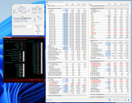
Tried to reduce SA, 1.12v failed on 1st VT3 loop, 1.14v on 3rd, 1.16 on 6th, didnt try 1.18v
Tried to reduce MC, 1.365, 1.375, 1.3825, 1.40 all failed on 1st loop
BUT i also tried TX/VDDQ at 1.22/1.46 and it passed 15 loops
Update: Boot pc today with TX/VDDQ 1.22/1.46 and freeze in windows, tried 1.21 didnt boot, 1.23 Karhu failed at 190%, 1.24 at 254%, tried 1.22 again pass 3000%. Turn off pc, come back home after 5 hours, start pc and freeze in windows within minutes. TX/VDDQ 1.25/1.48 seems tonally stable atm, pass both Karhu 7000% and 15 loops.
I also tried 8200C36 with the timings/voltages exactly as you suggested, it failed VT3 on 1st loop and Karhu at 550%. Maybe need more SA/MC?
Also 8400 mit 48gb mit CPU Oc funktioniert nur bis zum Ausschalter dann verstellt sich etwas und hab keine Lust mehr jeden Start das neu anzupassen
bin jetzt runter auf 8200 und es läuft mit CPU Oc
Hab das mit 8400 mit xmp Profil getestet was bei mir auf mb drauf ist hat aber das selbe verhalten
ohne CPU OC funktioniert 8400
Ich warte auf neue bios dann Versuch ist es nochmal
Lg haut rein
Ich kann dir nicht genau sagen ob es wegen dem Thermal Throttle ist
Oder du voltage Throttlest
Aber TX 1.2 war bei dir langsamer als 1.15v
Selbst wenn 1.15 dennoch irgendwie unstabil waren (SA zu hoch?)
Ich hatte es komplett verpeilt
VDDQ_CPU sollte kaum bis garnicht unter SA sein.
Wir rannten hier 1.25v SA auf 1.2-1.15v VDDQ_CPU.
Es ist selbstverständlich dass es irgendwann , nun instabil wird
habe jetzt mal SA auf 1.16v und den Rest gleich gelassen (TX 1.2 MC 1.4375 VDD/VDDQ 1.4) bei 8000
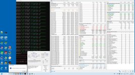
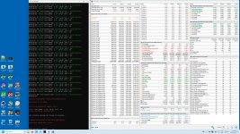
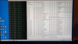
TM5 ist zumindest mal 90 min durchgelaufen, mal sehen was Karhu sagt....
habe jetzt mal SA auf 1.16v und den Rest gleich gelassen (TX 1.2 MC 1.4375 VDD/VDDQ 1.4) bei 8000
TM5 ist zumindest mal 90 min durchgelaufen, mal sehen was Karhu sagt....
Bug, hab ich bei anderen Usern auch schon gesehen. Frag mich aber auch warum das manchmal so ist. Sind definitiv 2 Riegel drin und werden erkannt und auch benutzt.
Ähnlich wie tWR exisiert der Wert tRTP welcher dort und auch im BIOS angezeigt wird eigentlich nicht, Intel CPUs haben keine Verwendung für diese Angabe. tWRPRE wäre hier ausschlaggebend, 23 wäre in dem Fall aber möglich.

.

")
")
")