Du verwendest einen veralteten Browser. Es ist möglich, dass diese oder andere Websites nicht korrekt angezeigt werden. Du solltest ein Upgrade durchführen oder einen alternativen Browser verwenden.
Sorry, Schwartz, aber egal denke ich.
Ich werde irgendwann den Kühler abbauen. Vielleich ich habe etwas falsch gebaut. Ich habe noch einen 13700k, tausche ich ihn auch für kurze Test.
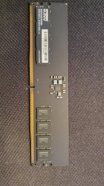
Ich bin neu mit ddr5, aber erste Tag als ich es gekauft und gebaut habe, geschafft 8200mhz. OK, nur TM5, aber zwei Stunde. Timing bestimmt schlegt, kopiert von Jemand, aber es ging. 8200/13700k
Mit 14900k und Wasserkühler geht garnichts.
Anhänge
754259_wtm0fcirocl4oadv_231218214427.jpg
104,9 KB
· Aufrufe: 128
754259_uuqzqusaect8dt8r_231218214401.jpg
79 KB
· Aufrufe: 123
754259_ugpvthanocdsmkyb_231218214457.jpg
75,7 KB
· Aufrufe: 115
754259_s8drmpdsvziulkpq_231218214333.jpg
71,1 KB
· Aufrufe: 127
20231113_063809.jpg
1,7 MB
· Aufrufe: 145
Wenn Du diese Anzeige nicht sehen willst, registriere Dich und/oder logge Dich ein.
G4 lief bei mir schon, mit 7-7.4GHz. Aber auf Stabilität habe ich es nicht getestet.
Wahrscheinlich sind NonK CPU's eher Nebenerscheinungen für dich, doch ich mag den kleinen Rebell
Meine Frage bezog sich auf den niedrigen Schwellenwert des SA. Ob ich mit meiner eingeschränkten CPU (angeblich max. 0,93 SA) über 7,6Ghz kommen kann.
Auf hwbot war die bisher maximale Ram Frequenz, bei übertakteter i5-12400 nonK: 7,516GHz.
Auf Stock habe ich die 12400 bereits mit 0,99 SA auf 7600Ghz zum laufen bekommen und lote jetzt aus, wie weit ich mit übertakteter CPU gehen kann.
Aktuell bin ich bei 7000GHz und der Ram will jetzt schon 1,47 VDD. Morgen versuche ich dann auf 7.2Ghz gehen, bis ich, wie ich hoffe auf 7.56GHz oder mehr landen kann.
Im Web waren bisher nur Gerüchte, darüber, dass höhere Frequenzen (8000/8200/8500) möglich sind.
Sorry, Schwartz, aber egal denke ich.
Ich werde irgendwann den Kühler abbauen. Vielleich ich habe etwas falsch gebaut. Ich habe noch einen 13700k, tausche ich ihn auch für kurze Test.
Ich bin neu mit ddr5, aber erste Tag als ich es gekauft und gebaut habe, geschafft 8200mhz. OK, nur TM5, aber zwei Stunde. Timing bestimmt schlegt, kopiert von Jemand, aber es ging. 8200/13700k
Mit 14900k und Wasserkühler geht garnichts.
This chip is , ehmm
If i wouldnt have seen worse ~ this would take first place.
On the most leakiest substrates. Potentially wonderful for SubZero & 1.6 vcore.
How can it be thaat bad.
Sorry for not being encouraging.
But this one will eat voltage. All of them
Meanwhile you try to undervolt
Now i understand :')
For the curve it needs 100mV Vcore more @ same clock, vs "normal" samples.
Wanna be silly for a sec ?
For a test ?
Ich hatte vermutet, dass es bei dir außerhalb des Bubble lag ;-)
Checke fast gar nix vom Ram OC. Dann muss der eben gute, alte logische Verstand herhalten
Beitrag automatisch zusammengeführt:
Ist es technisch möglich mit Class A, A-Dies, mit einer maximalen SA von 0.99V die 7600MHZ zu überschreiten? Und sagen wir Mal 7.7GHz oder gar 8GHz zu erreichen?
This chip is , ehmm
If i wouldnt have seen worse ~ this would take first place.
On the most leakiest substrates. Potentially wonderful for SubZero & 1.6 vcore.
How can it be thaat bad.
Sorry for not being encouraging.
But this one will eat voltage. All of them
Meanwhile you try to undervolt
Now i understand :')
For the curve it needs 100mV Vcore more @ same clock, vs "normal" samples.
Wanna be silly for a sec ?
For a test ?
Ich weiss, klumpest cpu auf der Welt. Aber nur solche können wir hier in Ungarn kaufen. Viele Freund hat gleiche.
Usa gebinnt, schlegt, neu verpack, "es ist gut für ost eu Lander..."
Schaut so aus.
OCn habe ich ein excel Tabelle gesehen von 100 cpu. Dast ist letzte von letzten...
Ich lache schon, weil weinen will ich nicht.
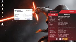
Timings hin oder her....es läuft. Muss mal diesem mix vt3/vst testen. Bin gerade auf Lan und hab mal die kurze Spielpause genutzt ^^. Anhang anzeigen 955752
Beitrag automatisch zusammengeführt:
1h vst auf dem UX 8200c34. Anhang anzeigen 955762
Hab den Rechner aber teils noch nebenher genutzt.... aber schön war das nicht ^^. Ladezeiten waren grausig.
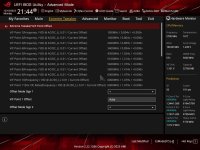
[2024/01/05 07:00:56]
Ai Overclock Tuner [Auto]
Intel(R) Adaptive Boost Technology [Auto]
ASUS MultiCore Enhancement [Auto – Lets BIOS Optimize]
SVID Behavior [Auto]
BCLK Frequency : DRAM Frequency Ratio [100:100]
Memory Controller : DRAM Frequency Ratio [1:2]
DRAM Frequency [DDR5-7600MHz]
Performance Core Ratio [Auto]
Performance Core0 Specific Ratio Limit [Auto]
Performance Core0 specific Voltage [Auto]
Performance Core1 Specific Ratio Limit [Auto]
Performance Core1 specific Voltage [Auto]
*Performance Core2 Specific Ratio Limit [Auto]
Performance Core2 specific Voltage [Auto]
*Performance Core3 Specific Ratio Limit [Auto]
Performance Core3 specific Voltage [Auto]
Performance Core4 Specific Ratio Limit [Auto]
Performance Core4 specific Voltage [Auto]
Performance Core5 Specific Ratio Limit [Auto]
Performance Core5 specific Voltage [Auto]
Performance Core6 Specific Ratio Limit [Auto]
Performance Core6 specific Voltage [Auto]
Performance Core7 Specific Ratio Limit [Auto]
Performance Core7 specific Voltage [Auto]
Efficient Core Ratio [Auto]
Efficient Core Group0 Specific Ratio Limit [45]
Efficient Core Group0 specific Voltage [Auto]
Efficient Core Group1 Specific Ratio Limit [45]
Efficient Core Group1 specific Voltage [Auto]
Efficient Core Group2 Specific Ratio Limit [45]
Efficient Core Group2 specific Voltage [Auto]
Efficient Core Group3 Specific Ratio Limit [45]
Efficient Core Group3 specific Voltage [Auto]
AVX2 [Enabled]
AVX2 Ratio Offset to per-core Ratio Limit [User Specify]
AVX2 Ratio Offset [0]
AVX2 Voltage Guardband Scale Factor [User Specify]
AVX2 Voltage Guardband Scale Factor [0]
Maximus Tweak [Mode 2]
DRAM CAS# Latency [34]
DRAM RAS# to CAS# Delay Read [44]
DRAM RAS# to CAS# Delay Write [44]
DRAM RAS# PRE Time [44]
DRAM RAS# ACT Time [56]
DRAM Command Rate [2N]
DRAM RAS# to RAS# Delay L [12]
DRAM RAS# to RAS# Delay S [8]
DRAM REF Cycle Time 2 [480]
DRAM REF Cycle Time Same Bank [Auto]
DRAM Refresh Interval [131071]
DRAM WRITE Recovery Time [Auto]
DRAM READ to PRE Time [12]
DRAM FOUR ACT WIN Time [32]
DRAM WRITE to READ Delay L [24]
DRAM WRITE to READ Delay S [8]
DRAM CKE Minimum Pulse Width [19]
DRAM Write Latency [32]
Ctl0 dqvrefup [162]
Ctl0 dqvrefdn [80]
Ctl0 dqodtvrefup [Auto]
Ctl0 dqodtvrefdn [Auto]
Ctl1 cmdvrefup [Auto]
Ctl1 ctlvrefup [Auto]
Ctl1 clkvrefup [Auto]
Ctl1 ckecsvrefup [Auto]
Ctl2 cmdvrefdn [Auto]
Ctl2 ctlvrefdn [Auto]
Ctl2 clkvrefdn [Auto]
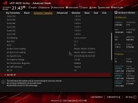
Read Equalization RxEq Start Sign [-]
Read Equalization RxEq Start [Auto]
Read Equalization RxEq Stop Sign [-]
Read Equalization RxEq Stop [Auto]
ODT_READ_DURATION [Auto]
ODT_READ_DELAY [Auto]
ODT_WRITE_DURATION [Auto]
ODT_WRITE_DELAY [Auto]
DQ RTT WR [40 DRAM Clock]
DQ RTT NOM RD [40 DRAM Clock]
DQ RTT NOM WR [40 DRAM Clock]
DQ RTT PARK [34 DRAM Clock]
DQ RTT PARK DQS [34 DRAM Clock]
GroupA CA ODT [240 DRAM Clock]
GroupA CS ODT [0 DRAM Clock]
GroupA CK ODT [0 DRAM Clock]
GroupB CA ODT [60 DRAM Clock]
GroupB CS ODT [40 DRAM Clock]
GroupB CK ODT [40 DRAM Clock]
Pull-up Output Driver Impedance [34 DRAM Clock]
Pull-Down Output Driver Impedance [34 DRAM Clock]
Round Trip Latency Init Value MC0 CHA [Auto]
Round Trip Latency Max Value MC0 CHA [Auto]
Round Trip Latency Offset Value Mode Sign MC0 CHA [-]
Round Trip Latency Offset Value MC0 CHA [Auto]
Round Trip Latency Init Value MC0 CHB [Auto]
Round Trip Latency Max Value MC0 CHB [Auto]
Round Trip Latency Offset Value Mode Sign MC0 CHB [-]
Round Trip Latency Offset Value MC0 CHB [Auto]
Round Trip Latency Init Value MC1 CHA [Auto]
Round Trip Latency Max Value MC1 CHA [Auto]
Round Trip Latency Offset Value Mode Sign MC1 CHA [-]
Round Trip Latency Offset Value MC1 CHA [Auto]
Round Trip Latency Init Value MC1 CHB [Auto]
Round Trip Latency Max Value MC1 CHB [Auto]
Round Trip Latency Offset Value Mode Sign MC1 CHB [-]
Round Trip Latency Offset Value MC1 CHB [Auto]
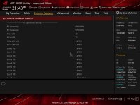
Round Trip Latency MC0 CHA R0 [Auto]
Round Trip Latency MC0 CHA R1 [Auto]
Round Trip Latency MC0 CHA R2 [0]
Round Trip Latency MC0 CHA R3 [0]
Round Trip Latency MC0 CHA R4 [0]
Round Trip Latency MC0 CHA R5 [0]
Round Trip Latency MC0 CHA R6 [0]
Round Trip Latency MC0 CHA R7 [0]
Round Trip Latency MC0 CHB R0 [Auto]
Round Trip Latency MC0 CHB R1 [Auto]
Round Trip Latency MC0 CHB R2 [0]
Round Trip Latency MC0 CHB R3 [0]
Round Trip Latency MC0 CHB R4 [0]
Round Trip Latency MC0 CHB R5 [0]
Round Trip Latency MC0 CHB R6 [0]
Round Trip Latency MC0 CHB R7 [0]
Round Trip Latency MC1 CHA R0 [Auto]
Round Trip Latency MC1 CHA R1 [Auto]
Round Trip Latency MC1 CHA R2 [0]
Round Trip Latency MC1 CHA R3 [0]
Round Trip Latency MC1 CHA R4 [0]
Round Trip Latency MC1 CHA R5 [0]
Round Trip Latency MC1 CHA R6 [0]
Round Trip Latency MC1 CHA R7 [0]
Round Trip Latency MC1 CHB R0 [Auto]
Round Trip Latency MC1 CHB R1 [Auto]
Round Trip Latency MC1 CHB R2 [0]
Round Trip Latency MC1 CHB R3 [0]
Round Trip Latency MC1 CHB R4 [0]
Round Trip Latency MC1 CHB R5 [0]
Round Trip Latency MC1 CHB R6 [0]
Round Trip Latency MC1 CHB R7 [0]
Early Command Training [Auto]
SenseAmp Offset Training [Auto]
Early ReadMPR Timing Centering 2D [Auto]
Read MPR Training [Auto]
Receive Enable Training [Auto]
Jedec Write Leveling [Auto]
Early Write Time Centering 2D [Auto]
Early Read Time Centering 2D [Auto]
Write Timing Centering 1D [Auto]
Write Voltage Centering 1D [Auto]
Read Timing Centering 1D [Auto]
Read Timing Centering with JR [Auto]
Dimm ODT Training* [Disabled]
Max RTT_WR [ODT Off]
DIMM RON Training* [Disabled]
Write Drive Strength/Equalization 2D* [Auto]
Write Slew Rate Training* [Auto]
Read ODT Training* [Disabled]
Comp Optimization Training [Auto]
Read Equalization Training* [Auto]
Read Amplifier Training* [Auto]
Write Timing Centering 2D [Auto]
Read Timing Centering 2D [Auto]
Command Voltage Centering [Auto]
Early Command Voltage Centering [Auto]
Write Voltage Centering 2D [Auto]
Read Voltage Centering 2D [Auto]
Late Command Training [Auto]
Round Trip Latency [Auto]
Turn Around Timing Training [Auto]
CMD CTL CLK Slew Rate [Auto]
CMD/CTL DS & E 2D [Auto]
Read Voltage Centering 1D [Auto]
TxDqTCO Comp Training* [Auto]
ClkTCO Comp Training* [Auto]
TxDqsTCO Comp Training* [Auto]
VccDLL Bypass Training [Auto]
CMD/CTL Drive Strength Up/Dn 2D [Auto]
DIMM CA ODT Training [Auto]
PanicVttDnLp Training* [Auto]
Read Vref Decap Training* [Auto]
Vddq Training [Disabled]
Duty Cycle Correction Training [Auto]
Periodic DCC [Auto]
Rank Margin Tool Per Bit [Auto]
DIMM DFE Training [Auto]
EARLY DIMM DFE Training [Auto]
Tx Dqs Dcc Training [Auto]
DRAM DCA Training [Auto]
Write Driver Strength Training [Auto]
Rank Margin Tool [Auto]
Memory Test [Auto]
DIMM SPD Alias Test [Auto]
Receive Enable Centering 1D [Auto]
Retrain Margin Check [Auto]
Write Drive Strength Up/Dn independently [Auto]
LPDDR DqDqs Re-Training [Auto]
Margin Check Limit [Disabled]
tRDRD_sg_Training [Auto]
tRDRD_sg_Runtime [16]
tRDRD_dg_Training [Auto]
tRDRD_dg_Runtime [8]
tRDWR_sg [20]
tRDWR_dg [20]
tWRWR_sg [16]
tWRWR_dg [8]
tWRRD_sg [Auto]
tWRRD_dg [Auto]
tRDRD_dr [0]
tRDRD_dd [Auto]
tRDWR_dr [0]
tRDWR_dd [Auto]
tWRWR_dr [0]
tWRWR_dd [Auto]
tWRRD_dr [0]
tWRRD_dd [Auto]
tRPRE [Auto]
tWPRE [Auto]
tWPOST [Auto]
tWRPRE [64]
tPRPDEN [2]
tRDPDEN [43]
tWRPDEN [65]
tCPDED [19]
tREFIX9 [Auto]
Ref Interval [Auto]
tXPDLL [Auto]
tXP [29]
tPPD [2]
tCCD_L_tDLLK [Auto]
tZQCAL [Auto]
tZQCS [Auto]
OREF_RI [Auto]
Refresh Watermarks [High]
Refresh Hp Wm [Auto]
Refresh Panic Wm [Auto]
Refresh Abr Release [Auto]
tXSDLL [2559]
tZQOPER [Auto]
tMOD [Auto]
CounttREFIWhileRefEn [Auto]
HPRefOnMRS [Auto]
SRX Ref Debits [Auto]
RAISE BLK WAIT [Auto]
Ref Stagger En [Auto]
Ref Stagger Mode [Auto]
Disable Stolen Refresh [Auto]
En Ref Type Display [Auto]
Trefipulse Stagger Disable [Auto]
tRPab ext [Auto]
derating ext [Auto]
Allow 2cyc B2B LPDDR [Auto]
tCSH [Auto]
tCSL [Auto]
powerdown Enable [Auto]
idle length [Auto]
raise cke after exit latency [Auto]
powerdown latency [Auto]
powerdown length [Auto]
selfrefresh latency [Auto]
selfrefresh length [Auto]
ckevalid length [Auto]
ckevalid enable [Auto]
idle enable [Auto]
selfrefresh enable [Auto]
Address mirror [Auto]
no gear4 param divide [Auto]
x8 device [Auto]
no gear2 param divide [Auto]
ddr 1dpc split ranks on subch [Auto]
write0 enable [Auto]
MultiCycCmd [Auto]
WCKDiffLowInIdle [Auto]
PBR Disable [Auto]
PBR OOO Dis [Auto]
PBR Disable on hot [Auto]
PBR Exit on Idle Cnt [Auto]
tXSR [645]
Dec tCWL [Auto]
Add tCWL [Auto]
Add 1Qclk delay [Auto]
MRC Fast Boot [Disabled]
MCH Full Check [Enabled]
Mem Over Clock Fail Count [2]
Training Profile [Auto]
RxDfe [Auto]
Mrc Training Loop Count [2]
DRAM CLK Period [Auto]
Dll_bwsel [Auto]
Controller 0, Channel 0 Control [Enabled]
Controller 0, Channel 1 Control [Enabled]
Controller 1, Channel 0 Control [Enabled]
Controller 1, Channel 1 Control [Enabled]
MC_Vref0 [Auto]
MC_Vref1 [Auto]
MC_Vref2 [Auto]
Fine Granularity Refresh mode [Auto]
SDRAM Density Per Die [Auto]
SDRAM Banks Per Bank Group [Auto]
SDRAM Bank Groups [Auto]
Dynamic Memory Boost [Disabled]
Realtime Memory Frequency [Disabled]
SA GV [Disabled]
Voltage Monitor [Die Sense]
VRM Initialization Check [Enabled]
CPU Input Voltage Load-line Calibration [Auto]
CPU Load-line Calibration [Auto]
Synch ACDC Loadline with VRM Loadline [Disabled]
CPU Current Capability [Auto]
CPU Current Reporting [Auto]
Core Voltage Suspension [Auto]
CPU VRM Switching Frequency [Auto]
VRM Spread Spectrum [Auto]
CPU Power Duty Control [Auto]
CPU Power Phase Control [Auto]
CPU Power Thermal Control [125]
CPU Core/Cache Boot Voltage [Auto]
CPU Input Boot Voltage [Auto]
PLL Termination Boot Voltage [Auto]
CPU Standby Boot Voltage [Auto]
Memory Controller Boot Voltage [Auto]
CPU Core Auto Voltage Cap [Auto]
CPU Input Auto Voltage Cap [Auto]
Memory Controller Auto Voltage Cap [Auto]
Maximum CPU Core Temperature [95]
Fast Throttle Threshold [Auto]
Package Temperature Threshold [Auto]
Regulate Frequency by above Threshold [Auto]
IVR Transmitter VDDQ ICCMAX [Auto]
Unlimited ICCMAX [Auto]
CPU Core/Cache Current Limit Max. [420.00]
Long Duration Package Power Limit [4095]
Package Power Time Window [Auto]
Short Duration Package Power Limit [4095]
Dual Tau Boost [Disabled]
IA AC Load Line [0.10]
IA DC Load Line [Auto]
IA CEP Enable [Disabled]
SA CEP Enable [Disabled]
IA SoC Iccmax Reactive Protector [Auto]
Inverse Temperature Dependency Throttle [Auto]
IA VR Voltage Limit [1700]
CPU SVID Support [Auto]
Cache Dynamic OC Switcher [Disabled]
TVB Voltage Optimizations [Disabled]
Enhanced TVB [Disabled]
Overclocking TVB [Disabled]
Overclocking TVB Global Temperature Offset Sign [+]
Overclocking TVB Global Temperature Offset Value [Auto]
Offset Mode Sign 1 [+]
V/F Point 1 Offset [Auto]
Offset Mode Sign 2 [+]
V/F Point 2 Offset [Auto]
Offset Mode Sign 3 [+]
V/F Point 3 Offset [Auto]
Offset Mode Sign 4 [+]
V/F Point 4 Offset [Auto]
Offset Mode Sign 5 [+]
V/F Point 5 Offset [Auto]
Offset Mode Sign 6 [+]
V/F Point 6 Offset [Auto]
Offset Mode Sign 7 [+]
V/F Point 7 Offset [Auto]
Offset Mode Sign 8 [+]
V/F Point 8 Offset [Auto]
Offset Mode Sign 9 [+]
V/F Point 9 Offset [Auto]
Offset Mode Sign 10 [+]
V/F Point 10 Offset [Auto]
Offset Mode Sign 11 [+]
V/F Point 11 Offset [Auto]
Initial BCLK Frequency [Auto]
Runtime BCLK OC [Auto]
BCLK Amplitude [Auto]
BCLK Slew Rate [Auto]
BCLK Spread Spectrum [Auto]
Initial PCIE Frequency [Auto]
PCIE/DMI Amplitude [Auto]
PCIE/DMI Slew Rate [Auto]
PCIE/DMI Spread Spectrum [Auto]
Cold Boot PCIE Frequency [Auto]
Realtime Memory Timing [Disabled]
SPD Write Disable [TRUE]
PVD Ratio Threshold [Auto]
SA PLL Frequency Override [Auto]
BCLK TSC HW Fixup [Enabled]
Core Ratio Extension Mode [Disabled]
FLL OC mode [Auto]
UnderVolt Protection [Disabled]
Switch Microcode [Current Microcode]
Xtreme Tweaking [Disabled]
Core PLL Voltage [Auto]
GT PLL Voltage [Auto]
Ring PLL Voltage [Auto]
System Agent PLL Voltage [Auto]
Memory Controller PLL Voltage [Auto]
Efficient-core PLL Voltage [Auto]
CPU 1.8V Small Rail [Auto]
PLL Termination Voltage [Auto]
CPU Standby Voltage [Auto]
PCH 1.05V Voltage [Auto]
PCH 0.82V Voltage [Auto]
CPU Input Voltage Reset Voltage [1.90000]
Eventual CPU Input Voltage [Auto]
Eventual Memory Controller Voltage [Auto]
Package Temperature Threshold [Auto]
Regulate Frequency by above Threshold [Auto]
Cooler Efficiency Customize [Keep Training]
Cooler Re-evaluation Algorithm [Normal]
Optimism Scale [100]
Ring Down Bin [Auto]
Min. CPU Cache Ratio [Auto]
Max. CPU Cache Ratio [Auto]
BCLK Aware Adaptive Voltage [Auto]
Actual VRM Core Voltage [Auto]
Global Core SVID Voltage [Auto]
Cache SVID Voltage [Auto]
CPU L2 Voltage [Auto]
CPU System Agent Voltage [Manual Mode]
- CPU System Agent Voltage Override [1.32000]
CPU Input Voltage [Auto]
High DRAM Voltage Mode [Enabled]
DRAM VDD Voltage [1.55000]
DRAM VDDQ Voltage [1.48000]
IVR Transmitter VDDQ Voltage [1.42000]
Memory Controller Voltage [1.48125]
MC Voltage Calculation Voltage Base [Auto]
VDD Calculation Voltage Base [Auto]
PMIC Voltages [Auto]
PCI Express Native Power Management [Enabled]
Native ASPM [Disabled]
DMI Link ASPM Control [Disabled]
ASPM [Auto]
L1 Substates [Disabled]
DMI ASPM [Disabled]
DMI Gen3 ASPM [Disabled]
PEG - ASPM [Disabled]
PCI Express Clock Gating [Enabled]
Hardware Prefetcher [Enabled]
Adjacent Cache Line Prefetch [Enabled]
Intel (VMX) Virtualization Technology [Disabled]
Per P-Core Control [Disabled]
Per E-Core Control [Disabled]
Active Performance Cores [All]
Active Efficient Cores [All]
Hyper-Threading [Enabled]
Hyper-Threading of Core 0 [Enabled]
Hyper-Threading of Core 1 [Enabled]
Hyper-Threading of Core 2 [Enabled]
Hyper-Threading of Core 3 [Enabled]
Hyper-Threading of Core 4 [Enabled]
Hyper-Threading of Core 5 [Enabled]
Hyper-Threading of Core 6 [Enabled]
Hyper-Threading of Core 7 [Enabled]
Total Memory Encryption [Disabled]
Legacy Game Compatibility Mode [Disabled]
Boot performance mode [Auto]
Intel(R) SpeedStep(tm) [Enabled]
Intel(R) Speed Shift Technology [Enabled]
Intel(R) Turbo Boost Max Technology 3.0 [Enabled]
Turbo Mode [Enabled]
Acoustic Noise Mitigation [Disabled]
CPU C-states [Auto]
Thermal Monitor [Enabled]
Dual Tau Boost [Disabled]
VT-d [Disabled]
Memory Remap [Enabled]
Enable VMD controller [Enabled]
Map PCIE Storage under VMD [Disabled]
Map SATA Controller under VMD [Disabled]
M.2_1 Link Speed [Auto]
PCIEX16(G5)_1 Link Speed [Auto]
PCIEX16(G5)_2 Link Speed [Auto]
PCIEX1(G4) Link Speed [Auto]
PCIEX4(G4) Link Speed [Auto]
M.2_2 Link Speed [Auto]
DIMM.2_1 Link Speed [Auto]
DIMM.2_2 Link Speed [Auto]
SATA Controller(s) [Enabled]
Aggressive LPM Support [Disabled]
SMART Self Test [Enabled]
M.2_3 [Enabled]
M.2_3 Hot Plug [Disabled]
SATA6G_1 [Enabled]
SATA6G_1 Hot Plug [Disabled]
SATA6G_2 [Enabled]
SATA6G_2 Hot Plug [Disabled]
SATA6G_3 [Enabled]
SATA6G_3 Hot Plug [Disabled]
SATA6G_4 [Enabled]
SATA6G_4 Hot Plug [Disabled]
PTT [Enable]
Intel(R) Dynamic Tuning Technology [Disabled]
PCIE Tunneling over USB4 [Enabled]
Discrete Thunderbolt(TM) Support [Disabled]
Security Device Support [Enable]
SHA256 PCR Bank [Enabled]
Pending operation [None]
Platform Hierarchy [Enabled]
Storage Hierarchy [Enabled]
Endorsement Hierarchy [Enabled]
Physical Presence Spec Version [1.3]
Disable Block Sid [Disabled]
Password protection of Runtime Variables [Enable]
Above 4G Decoding [Enabled]
Resize BAR Support [Enabled]
SR-IOV Support [Disabled]
Legacy USB Support [Enabled]
XHCI Hand-off [Enabled]
SanDisk [Auto]
LAN_U32G2_1 [Enabled]
U32G1_E5 [Enabled]
U32G1_E6 [Enabled]
U32G1_E7 [Enabled]
U32G1_E8 [Enabled]
U32G2X2_C3 [Enabled]
U32G2_5 [Enabled]
U32G2_6 [Enabled]
U32G2_7 [Enabled]
U32G2_P8 [Enabled]
U32G2X2_C9 [Enabled]
U32G1_E1 [Enabled]
U32G1_E2 [Enabled]
U32G1_E3 [Enabled]
U32G1_E4 [Enabled]
Network Stack [Disabled]
Device [N/A]
Restore AC Power Loss [Power Off]
Max Power Saving [Disabled]
ErP Ready [Disabled]
Power On By PCI-E [Disabled]
Power On By RTC [Disabled]
USB Audio [Enabled]
Intel LAN [Enabled]
USB power delivery in Soft Off state (S5) [Disabled]
Connectivity mode (Wi-Fi & Bluetooth) [Disabled]
When system is in working state [All On]
Q-Code LED Function [POST Code Only]
When system is in sleep, hibernate or soft off states [All On]
M.2_2 Configuration [Auto]
ASMedia USB 3.2 Controller_U32G1_E12 [Enabled]
ASMedia USB 3.2 Controller_U32G1_E34 [Enabled]
GNA Device [Disabled]
ASMedia Storage Controller [Enabled]
Windows Hot-plug Notification [Disabled]
ASPM Support [Disabled]
CPU Temperature [Monitor]
CPU Package Temperature [Monitor]
MotherBoard Temperature [Monitor]
VRM Temperature [Monitor]
Chipset Temperature [Monitor]
T_Sensor Temperature [Monitor]
DIMM.2 Sensor 1 Temperature [Monitor]
DIMM.2 Sensor 2 Temperature [Monitor]
Water In T Sensor Temperature [Monitor]
Water Out T Sensor Temperature [Monitor]
DIMM A1 Temperature [Monitor]
DIMM B1 Temperature [Monitor]
CPU Fan Speed [Monitor]
CPU Optional Fan Speed [Monitor]
Chassis Fan 1 Speed [Monitor]
Chassis Fan 2 Speed [Monitor]
Chassis Fan 3 Speed [Monitor]
Water Pump+ Speed [Monitor]
AIO Pump Speed [Monitor]
Flow Rate [Monitor]
CPU Core Voltage [Monitor]
12V Voltage [Monitor]
5V Voltage [Monitor]
3.3V Voltage [Monitor]
Memory Controller Voltage [Monitor]
CPU Fan Q-Fan Control [DC Mode]
CPU Fan Profile [Standard]
CPU Fan Q-Fan Source [CPU]
CPU Fan Step Up [Level 0]
CPU Fan Step Down [Level 4]
CPU Fan Speed Low Limit [200 RPM]
Chassis Fan 1 Q-Fan Control [Auto Detect]
Chassis Fan 1 Profile [Standard]
Chassis Fan 1 Q-Fan Source [CPU]
Chassis Fan 1 Step Up [Level 0]
Chassis Fan 1 Step Down [Level 0]
Chassis Fan 1 Speed Low Limit [200 RPM]
Chassis Fan 2 Q-Fan Control [PWM Mode]
Chassis Fan 2 Profile [Standard]
Chassis Fan 2 Q-Fan Source [Chipset]
Chassis Fan 2 Step Up [Level 0]
Chassis Fan 2 Step Down [Level 4]
Chassis Fan 2 Speed Low Limit [200 RPM]
Chassis Fan 3 Q-Fan Control [DC Mode]
Chassis Fan 3 Profile [Silent]
Chassis Fan 3 Q-Fan Source [CPU]
Chassis Fan 3 Step Up [Level 0]
Chassis Fan 3 Step Down [Level 0]
Chassis Fan 3 Speed Low Limit [200 RPM]
Water Pump+ Q-Fan Control [PWM Mode]
Water Pump+ Profile [Manual]
Water Pump+ Q-Fan Source [CPU]
Water Pump+ Step Up [Level 0]
Water Pump+ Step Down [Level 4]
Water Pump+ Speed Low Limit [Ignore]
Water Pump+ Point4 Temperature [70]
Water Pump+ Point4 Duty Cycle (%) [100]
Water Pump+ Point3 Temperature [50]
Water Pump+ Point3 Duty Cycle (%) [85]
Water Pump+ Point2 Temperature [40]
Water Pump+ Point2 Duty Cycle (%) [80]
Water Pump+ Point1 Temperature [25]
Water Pump+ Point1 Duty Cycle (%) [60]
AIO Pump Q-Fan Control [Auto Detect]
AIO Pump Profile [Full Speed]
CPU Temperature LED Switch [Enabled]
Launch CSM [Disabled]
OS Type [Other OS]
Secure Boot Mode [Custom]
Fast Boot [Enabled]
Next Boot after AC Power Loss [Fast Boot]
Boot Logo Display [Auto]
POST Delay Time [3 sec]
Bootup NumLock State [On]
Wait For 'F1' If Error [Enabled]
Option ROM Messages [Force BIOS]
Interrupt 19 Capture [Disabled]
AMI Native NVMe Driver Support [Enabled]
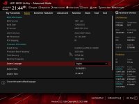
Setup Mode [Advanced Mode]
Boot Sector (MBR/GPT) Recovery Policy [Local User Control]
Next Boot Recovery Action [Skip]
BIOS Image Rollback Support [Enabled]
Publish HII Resources [Disabled]
Flexkey [Safe Boot]
Setup Animator [Disabled]
Load from Profile [4]
Profile Name [Veii7600]
Save to Profile [1]
DIMM Slot Number [DIMM_A1]
Download & Install ARMOURY CRATE app [Disabled]
Download & Install MyASUS service & app [Disabled]
Ich glaube, dass du nicht das sehen moechtest. Ich denke, dass ich die ganze Timing zueruckstellen sollte. Wenn nur 7600 ist ausgewaelt, Timings sind auf auto, kein boot. Egal ob MCH Fullcheck an oder aus, kein boot.
Es bootet nur, wenn ich ODTs + Timings manuell eingebe. Wenn ich nur Frequenz gebe, gehts nicht.
Als Spass kopiert Snakeeyes 8200 C34 46 46 mit meinem ODTs, bootet, aber Y Cruncher error.
MC 1.55V bootet auch
tRAS 59 or 60 - everything below is senseless. tRFC_pb can be tighter. RDRD_sg maybe 15, WRWR_dg 13 or 14. I'm curious to hear what veii says
Another question from my side... I can rund the same profile as posted ebove by Braegnok. And without any change (except RCD) also at 8400. Now the interesting part... tRCD 47 at 8266 is error free. So thats about 11,37ns. I would expect that tRCD 48 at 8400 is easy for the ICs then (11,42ns). But while the first one is stable, the latter can train and boot but errors out instantly in Karhu. So... is there any other timing involved or a dependency or may it be that the uneven values are just cosmetics and adressing is allways done on even values? I mean, is tRCD 47 set in reality an 48 - same as 48 set? And 49 set is 50 in reality?
Not much to change
tPPD 2 ~ 4 is a waste
RAS = RCD+X (12 here).
// RAS is a dynamic value, you only set the starting point. Instead of it repeating and fixing rowmisses, might as well get it correct~
RP never bellow RCD (47 or you push RCD down)
// RP happens in the background, so it shouldnt be your worry. If you see perf scaling - you have row-misses.
VDDQ_MEM 1.450
VDDQ_CPU 1.375 or 1.38
WRWR_SG never bellow RDRD_SG
Focus first on getting RCD 46 to run
later you can get RDWR_SG/DG lower if you really want.
Pushing there and not pushing on clock is kind of , suboptimal.
RCD happens on dimm
It doesnt bother if its 1N or 2N
CAS technically can be an odd value too ~ but here its different, because you have CPU communication
MEM strobe of 8
CPU strobe of 3 or 4
Needs alignment.
But CPU doesnt control RCD. SPD-HUB takes care of everything.
No need for rounding even with GearDownMode ~ which doesnt exist here.
CWL can be an odd value too.
Its also happening on dimm, outside of writes being twice as fast, as they don't have charge penalties & up to Arch design can happen at any time.
Most optimally two can happen per single read.
A single read can only happen in ticks of 8.
Even with individual "standalone" subchannel connection (arch + board design)
Internally on mem, it still needs 8 ticks to pass between actions (Read & WriteBurstlength ~ roundtrip is still 16. A Chop is just 8)
Only writes are speedup due to us (AMD/Intel) utilizing dimms differently.
Soo it doesnt matter if each subchannel is a single 32bit line, or we utilize how it should be to begin with, full 64bit "line" per dimm-side.
At the end you have DIMM PCB limitations. It doesnt matter what you as CPU Vendor try to do , or the user tries to achieve with too low timings.
And so on
While one Bank and one subchannel is busy
It doesnt mean that whole dimm is busy
It would be better illustration if i draw 4 + 4 ICs
And show that it roundrobin goes over all banks
Clock limit of 8 (well 16) is on the same location.
It doesnt mean that it can not start and prepare access to another bankgroup. (start and prepare doesnt mean success or active read)
and it doesnt mean that RAS2RAS (RRD) delay needs to be 8 to begin with
Its all depending on what type of data on what type of sorting (page size) is requested
// yet still chaining reads with low RRD_S, when the rest is unfinished is kind of a waste of power and increases volt requirements drastically
And then it depends if its a normal read, or this read needs to auto precharge its location after its done
needs to do, soo the next aligned and chained read has full charge and can access it
Yet for charging and for reading you need to protect the data you dont want to read and so destroy.
RCD here comes into play.
Because RCD has to elapse sooner or later
And AutoPreCh needs to run, any RAS associated READ ~ has to factor in to never be bellow RCD.
If it is, sooner or later a halting condition will happen
The same goes for RP. While that happens most optimally in the background
it makes no sense for it to be faster than RCD either.
Its there for repairing (2nd usecase) and for keeping cells charged
Moving data is also not indestructive. But reading is not full destructive. It only lets say 85-90% discharges target location
Memory itself has several methods to preserve charge and "keep alive" - like self refresh outside of having to hit RFC for either all banks ,, or RFC for separated per-bank
Huge huge topic
Lets end it here with:
"many operations are chained and aligned"
"Do not mess with order just because it allows you."
"You ruin efficiency that way"
Not much to change
tPPD 2 ~ 4 is a waste
RAS = RCD+X (12 here).
// RAS is a dynamic value, you only set the starting point. Instead of it repeating and fixing rowmisses, might as well get it correct~
RP never bellow RCD (47 or you push RCD down)
// RP happens in the background, so it shouldn't be your worry. If you see perf scaling - you have rows misses.
VDDQ_MEM 1,450
VDDQ_CPU 1.375 or 1.38
WRWR_SG never bellow RDRD_SG
Focus first on getting RCD 46 to run
later you can get RDWR_SG/DG lower if you really want.
Pushing there and not pushing on clock is kind of suboptimal.
Beitrag automatisch zusammengeführt:
RCD happens on dim
It doesn't bother if its 1N or 2N
CAS technically can be an odd value too ~ but here its different, because you have CPU communication
MEM strobe of 8
CPU strobe of 3 or 4
Needs alignment.
But CPU doesn't control RCD. SPD-HUB takes care of everything.
No need for rounding even with GearDownMode ~ which doesn't exist here.
CWL can be an odd value too.
Its also happening on dim, outside of writes being twice as fast, as they don't have charge penalties & up to Arch design can happen at any time.
Most optimally two can happen per single read.
A single read can only happen in ticks of 8.
Even with individual "standalone" subchannel connection (arch + board design)
Internally on mem, it still needs 8 ticks to pass between actions (Read & WriteBurstlength ~ roundtrip is still 16. A Chop is just 8)
Only writes are speedup due to us (AMD/Intel) utilizing dimms differently.
So it doesn't matter if each subchannel is a single 32bit line, or we utilize how it should be to begin with, full 64bit "line" per dimm-side.
At the end you have DIMM PCB limitations. It doesn't matter what you as CPU Vendor try to do, or the user tries to achieve with too low timings.
And so on
While one Bank and one subchannel is busy
It doesn't mean that whole dimming is busy
It would be better illustration if I drew 4 + 4 ICs
And show that it roundrobin goes over all banks
Clock limit of 8 (well 16) is on the same location.
It doesn't mean that it can't start and prepare access to another bankgroup. (start and prepare doesn't mean success or active read)
and it doesn't mean that RAS2RAS (RRD) delay needs to be 8 to begin with
Its all depending on what type of data on what type of sorting (page size) is requested
// yet still chaining reads with low RRD_S, when the rest is unfinished is kind of a waste of power and increases volt requirements dramatically
And then it depends if its a normal read, or this read needs to auto precharge its location after its done
needs to do, so the next aligned and chained read has full charge and can access it
Yet for charging and for reading you need to protect the data you don't want to read and so destroy.
RCD here comes into play.
Because RCD has to elapse sooner or later
And AutoPreCh needs to run, any RAS associated READ ~ has to factor in to never be bellow RCD.
If it is, sooner or later a halting condition will happen
The same goes for RP. While that happens most optimally in the background
it makes no sense for it to be faster than RCD either.
Its there for repairing (2nd usecase) and for keeping cells charged
Moving data is also not indestructive. But reading is not completely destructive. It only lets say 85-90% discharges target location
Memory itself has several methods to preserve charge and "keep alive" - like self refresh outside of having to hit RFC for either all banks ,, or RFC for separated per-bank
Huge topic
Let's end it here with:
"many operations are chained and aligned"
"Don't mess with order just because it allows you."
"You ruin efficiency that way"
@Veii habe deine Settings übernommen und die 8600 laufen soweit Karhu und 1Usmus stabil. Nur VT3+VST ist noch zickig. Mal läuft es 90min+ und mal nur 2 iterations.
Hast nen Tipp wo ich mal schauen oder testen kann? (Plls zb?)
tRFC Mini Anhang anzeigen 955440
I need to spend time and adhere to JEDEC committee's rounding math, but those are the values.
Never heard of "+1nCK over CKE". Am i missing something ?
Its raw, i blame myself for it
But it appeared useful and thought why not keep it
Select freq
Input manually your target RFC
view suggestion
It really has barely any love put in
But it works
Depends on RFC which gets converted to realtime-ns , added a distance offset , then back to nCK value.
I wouldnt call it JEDEC approved
Especially because whole docs needs a little remake to convert back and forth the JEDEC way ~ in picoseconds
But its functional so far, soo i'm kind of lazy
Also no system to use as testing rabbit.
Both Anhang anzeigen 956094
Its raw, i blame myself for it
But it appeared useful and thought why not keep it
Select freq
Input manually your target RFC
view suggestion
It really has barely any love put in
But it works
Depends on RFC which gets converted to realtime-ns , added a distance offset , then back to nCK value.
I wouldnt call it JEDEC approved
Especially because whole docs needs a little remake to convert back and forth the JEDEC way ~ in picoseconds
But its functional so far, soo i'm kind of lazy
Also no system to use as testing rabbit.

")
")
.png")
.png")


