zebra_hun
Profi
And OC Tool, too. I can't find... ThanksGibts die Excel irgendwo zum Download?
Follow along with the video below to see how to install our site as a web app on your home screen.

Anmerkung: this_feature_currently_requires_accessing_site_using_safari
And OC Tool, too. I can't find... ThanksGibts die Excel irgendwo zum Download?
And OC Tool, too. I can't find... Thanks
Core/memory isolation (antivirus) muss ausBraegnok, danke dir. Untrer W11 nicht funkzioniert, aber aufm W10 gehts.
Auto und TVB verwendenSo ist eingestellt:
2C 58x, 4C 57x, 6C 56x 8C 55x P
44x alle E Core
49x ist max Ring
0.3AC LL 0.01
- Global SVID = Trained.Core/memory isolation (antivirus) muss aus
Funktioniert gut.
Y-Cruncher SFT fürs core voltage testing.
Global SVID = Trained.
50mV ≠ 50mV
Du verschiebst die Kurve.
5800 punkt 8 peakt höher als Punkt 9-11
Punkt 9-11 wird somit ignoriert.
Auto und TVB verwenden
Kein fixierter clock und keine fixierte Spannung.
Ring ebenfalls auto
Hwinfo stört ASUS Tool.
Hat aus zu sein.
Beitrag automatisch zusammengeführt:
0.3
0.0X ist zu tief
Hm ?14900k allcore 5700MHz, und 2 o. 3 Kerne 60x. Es wird nie in Leben mit mein 6C Wasser gehen.
")
Bzw fals man V/F bis P5 oder sogar P3 fertig hat & weiterhin instabil ist ~ oder instabil bei höherem MemCLK wird:Sobald man 3-4 Stunden schafft, ins Bios zurück und IA LLC von 0.3 auf 0.28 dann 0.25 ~ und SFT nochmal für mindestens ne 90min gegentesten.
V/F curve nicht mehr anfassen.

Ich verstehe auch nicht wieso man sich auf irgendwelche Spannung fixiert.VID zu Diesense ist für dich interessant. Eigentlich nur VID & Rechenleistung.
Wattage ist unwichtig, effective clock ist unwichtig.
Die CPU throttled kostant, du möchtest die Curve tiefer bekommen damit sie weniger throttled und mehr max-IOPS "rauskommen".Versuche es zu lernenHoffentlich melde ich mich schnell. Es ist nicht 10 Minute. Total anders wie ich es in meinem Leben bis jetzt gemacht hab. Wirds schon gehen, danke.

Letzte Frage bevor ich "verschwunde" (es dauert viel Zeit) Welche Sicherung darf/kann ich nutzen?Versuche es zu lernen
So arbeiten Zen CPUs (etwas mehr variablen)
Und so arbeiten 12++ Gen, Intel CPUs.
Es wird nur komplexer, nicht einfacher.
AMD nutzt AVFS für alles, GPUs inclusive.
Manual "fixed" clock is dead since ~2014 🤭
12th gen hatte eigene V/F Punkte.
13/14th gen hat ein "highest voltage wins" System.
Hier muss man besonders bei der V/F curve aufpassen.
Kein Punkt in der mitte darf "als resultat, nicht als offset" ~ höher sein als der nächste Punkt
P6 1100mV
P7 1150
P8 1125
Darf nicht passieren !
P8 wird ignoriert und jeder Punkt drüber welcher "als Resultat !" weniger Spannung sich nimmt ~ wird ignoriert.
Siehe:
~ grobes Beispiel
Die Werte welche du eingibst sind "shifting-offsets"
Sie nehmen die Fused Curve und bewegen sie um X mV
Sie heißen nicht gleich mV. Sie sind nur offsets. Keine echte Spannung
Sobald du fertig bist,
Ist es egal welche Clock rennt. Sie wird sich nach dieser Curve orientieren.
Du musst dir viel mühe geben und verschiedene Lastarten testen, dass du kein negatives Scaling hast
Wenn die CPU dann merkt sie hat noch (A) & C° Headroom, wird sie höher boosten.
Es ist unwichtig welcher clock anliegt, aber wenn es unterhalb des Spannungslimits liegt, boostet sie höher.
Somit ist es wichtig, die gesammt Curve gut und niedrig hinbekommen. Dann kommen auch mehr MHz raus.
Oder minimum mehr IOPS pro MHz clock. Somit kann auch Ring selbstständig höher, sollte noch "headroom" bleiben.
, morgen werde ich draussen in Garten. Ich denke, dass cpu kuemmert sich um selbe, aber ich moechte alles einsichern.ASUS hat ein " unlimited Powerlimit, 90° " ~ Limiter PresetLetzte Frage bevor ich "verschwunde" (es dauert viel Zeit) Welche Sicherung darf/kann ich nutzen?
Amper auto oder 420A?
Temperature auto oder darf ich zB.: 95C eingeben?
PL1 u. 2 darf ich etwas eingeben, oder 4095W? Auto sind 4095, grrrr, das ist kein Sicherung.
Die Kerne sind auf auto. Boostet so hoch wie cpu will, ok.
Ich will nicht kochen auf dem Rechner
Noch etwas, sehr gutes Thema, aber es ist bischen weit weg von RAM OC, deswegen sorry fuer Forum. Vielleich nutzt noch es Jemend. Danke die viele gutes Infos
On 3rd test i changed TVB peak, (applied to 4th too)
 www.icemancooler.com
wo finde ich diese Tabelle? Kann ich da alles selber eingeben?
Actually interesting, but when using normal water coolers I currently always have a delta between water and ram temp of around 3-6 degrees. Does the Direct Die bring so much more?
And how “safe” is the seal between the cooler and the ram cover and how can the whole thing be removed without having bad luck leaving residues of the coolant running over the RAMs.
Is it already available to buy?
Do you have a link to the shop?
Edit:
ICE-RDT Direct touch RAM blocks
IceManCooler is a leading enterprise in the export and domestic production of computer, industrial water cooling equipment and precision hardware components. Main products: water cooling suit, water cooling head, water pump and parts, water tank, water flow meter, cold exhaust, water cooling...
Ich hab dir hier mal meine Eingaben, für 6800MHZ. Ich habe ein Z690 Formula. Sollte in etwa gleich sein wie dein HERO.wo finde ich diese Tabelle? Kann ich da alles selber eingeben?
Firstly thanks for all your Infomations here. Also I started from scratch my CPU and RAM OC, if i try 6600/6800 i get errors. I use Prime 95 Blend my workers Stopping/ + WHEA Error Cpu+ L2
With this Current Setup like this any tipps or improvements could you look maybe at my timings?
CPU is 13700K @ Best Case Scenario and -0.018 SVID on 5,5Ghz all Core and 4,3 E Core and 4,7 Ring. XMP I Loaded and tweaked by myself fully stable. In Aida ima between 59,3ns- 60,5
I Think im Cursed too my pc freezes randomly when i use ASRTC
meine v/f kurven sind standart im bios ka habe da gefummelt aber hat gefühlt nichts bewirkt?
ach wieso schreibe ich englisch du kannst doch deutsch xd
@Braegnok
Yeah, just read some posts in this thread and it seems that some people have problems with this block - leaking or quality issues with the screws.
But I am happy with my Bitspower cooler. "Direct die" is no opinion for me.


..welcome here@Veii
Just registered to say thank you for your work and suggestions.
Since you are not active on OCN I would like to share my latest profile here with you.
Timings are based on your TRFC Mini and suggestions,
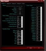
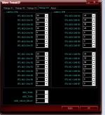
CPU is P59x3 58x5 57x8 E45 R45-50, LLC4 AC_ll 0.22 ICCMAX 420A
Dram VDD: 1.56V
Dram VDDQ: 1.45V
TX: 1.30V
MC: 1.50V
SA: 1.18V
Tank you. 😊..welcome here
..absolutely notTank you. 😊
Hope it's not a problem that I use English here.
Up to how much vdimm could you go with air? Now I have 1.4850v and the ram is about 32 degrees. I would like to have over 8000mhz but I only see over 1,500v for everything that is that high.
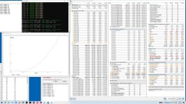
Es ist nicht so schlegt. Benched paar Benchmark auf diesem 24/7 Setup, ohne Tricks (HT Off usw.), zeigt gut. 280 min fps TR Bench, 180 min fps CP77, 45 sec 2.5b, finde ich gut. Ich schaue nur min fps.@Veii
Heute habe ich leider keine Zeit, aber schwer mich es nicht zu machen. Ganz kurz habe ich zwischen 51x-58x points fuer SFT ausgemacht. 8 Min lang getestet nur, aber wenn es fuer SFT stabil ist, dann genug fuer VST/VT3.
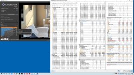
NvExperience schnell installiert, so konnte ich kurz Video machen. Besser wie einen Bild.
Video
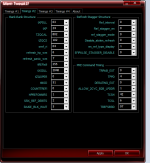
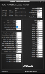
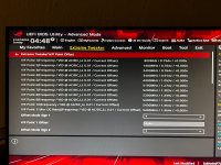
[2024/01/07 13:12:25]
Ai Overclock Tuner [Auto]
Intel(R) Adaptive Boost Technology [Auto]
ASUS MultiCore Enhancement [Enabled – Remove All limits (90°C)]
SVID Behavior [Trained]
BCLK Frequency : DRAM Frequency Ratio [100:100]
Memory Controller : DRAM Frequency Ratio [1:2]
DRAM Frequency [DDR5-7200MHz]
Performance Core Ratio [Auto]
Performance Core0 Specific Ratio Limit [Auto]
Performance Core0 specific Voltage [Auto]
Performance Core1 Specific Ratio Limit [Auto]
Performance Core1 specific Voltage [Auto]
*Performance Core2 Specific Ratio Limit [Auto]
Performance Core2 specific Voltage [Auto]
*Performance Core3 Specific Ratio Limit [Auto]
Performance Core3 specific Voltage [Auto]
Performance Core4 Specific Ratio Limit [Auto]
Performance Core4 specific Voltage [Auto]
Performance Core5 Specific Ratio Limit [Auto]
Performance Core5 specific Voltage [Auto]
Performance Core6 Specific Ratio Limit [Auto]
Performance Core6 specific Voltage [Auto]
Performance Core7 Specific Ratio Limit [Auto]
Performance Core7 specific Voltage [Auto]
Efficient Core Ratio [Auto]
Efficient Core Group0 Specific Ratio Limit [Auto]
Efficient Core Group0 specific Voltage [Auto]
Efficient Core Group1 Specific Ratio Limit [Auto]
Efficient Core Group1 specific Voltage [Auto]
Efficient Core Group2 Specific Ratio Limit [Auto]
Efficient Core Group2 specific Voltage [Auto]
Efficient Core Group3 Specific Ratio Limit [Auto]
Efficient Core Group3 specific Voltage [Auto]
AVX2 [Auto]
AVX2 Ratio Offset to per-core Ratio Limit [Auto]
AVX2 Voltage Guardband Scale Factor [Auto]
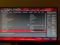
Maximus Tweak [Mode 2]
DRAM CAS# Latency [32]
DRAM RAS# to CAS# Delay Read [42]
DRAM RAS# to CAS# Delay Write [16]
DRAM RAS# PRE Time [42]
DRAM RAS# ACT Time [54]
DRAM Command Rate [2N]
DRAM RAS# to RAS# Delay L [12]
DRAM RAS# to RAS# Delay S [8]
DRAM REF Cycle Time 2 [448]
DRAM REF Cycle Time Same Bank [Auto]
DRAM Refresh Interval [131071]
DRAM WRITE Recovery Time [24]
DRAM READ to PRE Time [12]
DRAM FOUR ACT WIN Time [32]
DRAM WRITE to READ Delay L [24]
DRAM WRITE to READ Delay S [10]
DRAM CKE Minimum Pulse Width [Auto]
DRAM Write Latency [30]
Ctl0 dqvrefup [154]
Ctl0 dqvrefdn [72]
Ctl0 dqodtvrefup [Auto]
Ctl0 dqodtvrefdn [Auto]
Ctl1 cmdvrefup [Auto]
Ctl1 ctlvrefup [Auto]
Ctl1 clkvrefup [Auto]
Ctl1 ckecsvrefup [Auto]
Ctl2 cmdvrefdn [Auto]
Ctl2 ctlvrefdn [Auto]
Ctl2 clkvrefdn [Auto]
Read Equalization RxEq Start Sign [-]
Read Equalization RxEq Start [Auto]
Read Equalization RxEq Stop Sign [-]
Read Equalization RxEq Stop [Auto]
ODT_READ_DURATION [Auto]
ODT_READ_DELAY [Auto]
ODT_WRITE_DURATION [Auto]
ODT_WRITE_DELAY [Auto]
DQ RTT WR [40 DRAM Clock]
DQ RTT NOM RD [40 DRAM Clock]
DQ RTT NOM WR [40 DRAM Clock]
DQ RTT PARK [34 DRAM Clock]
DQ RTT PARK DQS [34 DRAM Clock]
GroupA CA ODT [240 DRAM Clock]
GroupA CS ODT [0 DRAM Clock]
GroupA CK ODT [0 DRAM Clock]
GroupB CA ODT [60 DRAM Clock]
GroupB CS ODT [40 DRAM Clock]
GroupB CK ODT [40 DRAM Clock]
Pull-up Output Driver Impedance [34 DRAM Clock]
Pull-Down Output Driver Impedance [34 DRAM Clock]
Round Trip Latency Init Value MC0 CHA [Auto]
Round Trip Latency Max Value MC0 CHA [Auto]
Round Trip Latency Offset Value Mode Sign MC0 CHA [-]
Round Trip Latency Offset Value MC0 CHA [Auto]
Round Trip Latency Init Value MC0 CHB [Auto]
Round Trip Latency Max Value MC0 CHB [Auto]
Round Trip Latency Offset Value Mode Sign MC0 CHB [-]
Round Trip Latency Offset Value MC0 CHB [Auto]
Round Trip Latency Init Value MC1 CHA [Auto]
Round Trip Latency Max Value MC1 CHA [Auto]
Round Trip Latency Offset Value Mode Sign MC1 CHA [-]
Round Trip Latency Offset Value MC1 CHA [Auto]
Round Trip Latency Init Value MC1 CHB [Auto]
Round Trip Latency Max Value MC1 CHB [Auto]
Round Trip Latency Offset Value Mode Sign MC1 CHB [-]
Round Trip Latency Offset Value MC1 CHB [Auto]
Round Trip Latency MC0 CHA R0 [Auto]
Round Trip Latency MC0 CHA R1 [Auto]
Round Trip Latency MC0 CHA R2 [0]
Round Trip Latency MC0 CHA R3 [0]
Round Trip Latency MC0 CHA R4 [0]
Round Trip Latency MC0 CHA R5 [0]
Round Trip Latency MC0 CHA R6 [0]
Round Trip Latency MC0 CHA R7 [0]
Round Trip Latency MC0 CHB R0 [Auto]
Round Trip Latency MC0 CHB R1 [Auto]
Round Trip Latency MC0 CHB R2 [0]
Round Trip Latency MC0 CHB R3 [0]
Round Trip Latency MC0 CHB R4 [0]
Round Trip Latency MC0 CHB R5 [0]
Round Trip Latency MC0 CHB R6 [0]
Round Trip Latency MC0 CHB R7 [0]
Round Trip Latency MC1 CHA R0 [Auto]
Round Trip Latency MC1 CHA R1 [Auto]
Round Trip Latency MC1 CHA R2 [0]
Round Trip Latency MC1 CHA R3 [0]
Round Trip Latency MC1 CHA R4 [0]
Round Trip Latency MC1 CHA R5 [0]
Round Trip Latency MC1 CHA R6 [0]
Round Trip Latency MC1 CHA R7 [0]
Round Trip Latency MC1 CHB R0 [Auto]
Round Trip Latency MC1 CHB R1 [Auto]
Round Trip Latency MC1 CHB R2 [0]
Round Trip Latency MC1 CHB R3 [0]
Round Trip Latency MC1 CHB R4 [0]
Round Trip Latency MC1 CHB R5 [0]
Round Trip Latency MC1 CHB R6 [0]
Round Trip Latency MC1 CHB R7 [0]
Early Command Training [Auto]
SenseAmp Offset Training [Auto]
Early ReadMPR Timing Centering 2D [Auto]
Read MPR Training [Auto]
Receive Enable Training [Auto]
Jedec Write Leveling [Auto]
Early Write Time Centering 2D [Auto]
Early Read Time Centering 2D [Auto]
Write Timing Centering 1D [Auto]
Write Voltage Centering 1D [Auto]
Read Timing Centering 1D [Auto]
Read Timing Centering with JR [Auto]
Dimm ODT Training* [Disabled]
Max RTT_WR [ODT Off]
DIMM RON Training* [Disabled]
Write Drive Strength/Equalization 2D* [Auto]
Write Slew Rate Training* [Auto]
Read ODT Training* [Disabled]
Comp Optimization Training [Auto]
Read Equalization Training* [Auto]
Read Amplifier Training* [Auto]
Write Timing Centering 2D [Auto]
Read Timing Centering 2D [Auto]
Command Voltage Centering [Auto]
Early Command Voltage Centering [Auto]
Write Voltage Centering 2D [Auto]
Read Voltage Centering 2D [Auto]
Late Command Training [Auto]
Round Trip Latency [Auto]
Turn Around Timing Training [Auto]
CMD CTL CLK Slew Rate [Auto]
CMD/CTL DS & E 2D [Auto]
Read Voltage Centering 1D [Auto]
TxDqTCO Comp Training* [Auto]
ClkTCO Comp Training* [Auto]
TxDqsTCO Comp Training* [Auto]
VccDLL Bypass Training [Auto]
CMD/CTL Drive Strength Up/Dn 2D [Auto]
DIMM CA ODT Training [Auto]
PanicVttDnLp Training* [Auto]
Read Vref Decap Training* [Auto]
Vddq Training [Disabled]
Duty Cycle Correction Training [Auto]
Periodic DCC [Auto]
Rank Margin Tool Per Bit [Auto]
DIMM DFE Training [Auto]
EARLY DIMM DFE Training [Auto]
Tx Dqs Dcc Training [Auto]
DRAM DCA Training [Auto]
Write Driver Strength Training [Auto]
Rank Margin Tool [Auto]
Memory Test [Auto]
DIMM SPD Alias Test [Auto]
Receive Enable Centering 1D [Auto]
Retrain Margin Check [Auto]
Write Drive Strength Up/Dn independently [Auto]
LPDDR DqDqs Re-Training [Auto]
Margin Check Limit [Disabled]
tRDRD_sg_Training [Auto]
tRDRD_sg_Runtime [16]
tRDRD_dg_Training [Auto]
tRDRD_dg_Runtime [8]
tRDWR_sg [18]
tRDWR_dg [18]
tWRWR_sg [16]
tWRWR_dg [8]
tWRRD_sg [Auto]
tWRRD_dg [Auto]
tRDRD_dr [0]
tRDRD_dd [Auto]
tRDWR_dr [0]
tRDWR_dd [Auto]
tWRWR_dr [0]
tWRWR_dd [Auto]
tWRRD_dr [0]
tWRRD_dd [Auto]
tRPRE [Auto]
tWPRE [Auto]
tWPOST [Auto]
tWRPRE [Auto]
tPRPDEN [Auto]
tRDPDEN [Auto]
tWRPDEN [Auto]
tCPDED [Auto]
tREFIX9 [Auto]
Ref Interval [Auto]
tXPDLL [Auto]
tXP [Auto]
tPPD [Auto]
tCCD_L_tDLLK [Auto]
tZQCAL [Auto]
tZQCS [Auto]
OREF_RI [Auto]
Refresh Watermarks [High]
Refresh Hp Wm [Auto]
Refresh Panic Wm [Auto]
Refresh Abr Release [Auto]
tXSDLL [Auto]
tZQOPER [Auto]
tMOD [Auto]
CounttREFIWhileRefEn [Auto]
HPRefOnMRS [Auto]
SRX Ref Debits [Auto]
RAISE BLK WAIT [Auto]
Ref Stagger En [Auto]
Ref Stagger Mode [Auto]
Disable Stolen Refresh [Auto]
En Ref Type Display [Auto]
Trefipulse Stagger Disable [Auto]
tRPab ext [Auto]
derating ext [Auto]
Allow 2cyc B2B LPDDR [Auto]
tCSH [Auto]
tCSL [Auto]
powerdown Enable [Auto]
idle length [Auto]
raise cke after exit latency [Auto]
powerdown latency [Auto]
powerdown length [Auto]
selfrefresh latency [Auto]
selfrefresh length [Auto]
ckevalid length [Auto]
ckevalid enable [Auto]
idle enable [Auto]
selfrefresh enable [Auto]
Address mirror [Auto]
no gear4 param divide [Auto]
x8 device [Auto]
no gear2 param divide [Auto]
ddr 1dpc split ranks on subch [Auto]
write0 enable [Auto]
MultiCycCmd [Auto]
WCKDiffLowInIdle [Auto]
PBR Disable [Auto]
PBR OOO Dis [Auto]
PBR Disable on hot [Auto]
PBR Exit on Idle Cnt [Auto]
tXSR [Auto]
Dec tCWL [Auto]
Add tCWL [Auto]
Add 1Qclk delay [Auto]
MRC Fast Boot [Disabled]
MCH Full Check [Auto]
Mem Over Clock Fail Count [2]
Training Profile [Auto]
RxDfe [Auto]
Mrc Training Loop Count [2]
DRAM CLK Period [Auto]
Dll_bwsel [Auto]
Controller 0, Channel 0 Control [Enabled]
Controller 0, Channel 1 Control [Enabled]
Controller 1, Channel 0 Control [Enabled]
Controller 1, Channel 1 Control [Enabled]
MC_Vref0 [Auto]
MC_Vref1 [Auto]
MC_Vref2 [Auto]
Fine Granularity Refresh mode [Auto]
SDRAM Density Per Die [Auto]
SDRAM Banks Per Bank Group [Auto]
SDRAM Bank Groups [Auto]
Dynamic Memory Boost [Disabled]
Realtime Memory Frequency [Disabled]
SA GV [Disabled]
Voltage Monitor [Die Sense]
VRM Initialization Check [Enabled]
CPU Input Voltage Load-line Calibration [Auto]
CPU Load-line Calibration [Auto]
Synch ACDC Loadline with VRM Loadline [Disabled]
CPU Current Capability [Auto]
CPU Current Reporting [Auto]
Core Voltage Suspension [Auto]
CPU VRM Switching Frequency [Auto]
VRM Spread Spectrum [Auto]
CPU Power Duty Control [Auto]
CPU Power Phase Control [Auto]
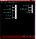
CPU Power Thermal Control [125]
CPU Core/Cache Boot Voltage [Auto]
CPU Input Boot Voltage [Auto]
PLL Termination Boot Voltage [Auto]
CPU Standby Boot Voltage [Auto]
Memory Controller Boot Voltage [Auto]
CPU Core Auto Voltage Cap [Auto]
CPU Input Auto Voltage Cap [Auto]
Memory Controller Auto Voltage Cap [Auto]
Fast Throttle Threshold [Auto]
Package Temperature Threshold [Auto]
Regulate Frequency by above Threshold [Auto]
IVR Transmitter VDDQ ICCMAX [Auto]
Unlimited ICCMAX [Auto]
CPU Core/Cache Current Limit Max. [420.00]
Long Duration Package Power Limit [Auto]
Package Power Time Window [Auto]
Short Duration Package Power Limit [Auto]
Dual Tau Boost [Disabled]
IA AC Load Line [0.30]
IA DC Load Line [Auto]
IA CEP Enable [Disabled]
SA CEP Enable [Disabled]
IA SoC Iccmax Reactive Protector [Auto]
Inverse Temperature Dependency Throttle [Auto]
IA VR Voltage Limit [1650]
CPU SVID Support [Auto]
Cache Dynamic OC Switcher [Auto]
TVB Voltage Optimizations [Enabled]
Enhanced TVB [Enabled]
Overclocking TVB [Boost Until Target]
Max Boost Target in MHz [Auto]
Overclocking TVB Global Temperature Offset Sign [+]
Overclocking TVB Global Temperature Offset Value [Auto]
Offset Mode Sign 1 [+]
V/F Point 1 Offset [Auto]
Offset Mode Sign 2 [+]
V/F Point 2 Offset [Auto]
Offset Mode Sign 3 [+]
V/F Point 3 Offset [Auto]
Offset Mode Sign 4 [+]
V/F Point 4 Offset [Auto]
Offset Mode Sign 5 [-]
V/F Point 5 Offset [0.01000]
Offset Mode Sign 6 [-]
V/F Point 6 Offset [0.02500]
Offset Mode Sign 7 [-]
V/F Point 7 Offset [0.02600]
Offset Mode Sign 8 [-]
V/F Point 8 Offset [0.02800]
Offset Mode Sign 9 [-]
V/F Point 9 Offset [0.03000]
Offset Mode Sign 10 [-]
V/F Point 10 Offset [0.03400]
Offset Mode Sign 11 [-]
V/F Point 11 Offset [0.03500]
Initial BCLK Frequency [Auto]
Runtime BCLK OC [Auto]
BCLK Amplitude [Auto]
BCLK Slew Rate [Auto]
BCLK Spread Spectrum [Auto]
Initial PCIE Frequency [Auto]
PCIE/DMI Amplitude [Auto]
PCIE/DMI Slew Rate [Auto]
PCIE/DMI Spread Spectrum [Auto]
Cold Boot PCIE Frequency [Auto]
Realtime Memory Timing [Disabled]
SPD Write Disable [TRUE]
PVD Ratio Threshold [Auto]
SA PLL Frequency Override [Auto]
BCLK TSC HW Fixup [Enabled]
Core Ratio Extension Mode [Disabled]
FLL OC mode [Auto]
UnderVolt Protection [Disabled]
Switch Microcode [Current Microcode]
Xtreme Tweaking [Disabled]
Core PLL Voltage [Auto]
GT PLL Voltage [Auto]
Ring PLL Voltage [Auto]
System Agent PLL Voltage [Auto]
Memory Controller PLL Voltage [Auto]
Efficient-core PLL Voltage [Auto]
CPU 1.8V Small Rail [Auto]
PLL Termination Voltage [Auto]
CPU Standby Voltage [Auto]
PCH 1.05V Voltage [Auto]
PCH 0.82V Voltage [Auto]
CPU Input Voltage Reset Voltage [Auto]
Eventual CPU Input Voltage [Auto]
Eventual Memory Controller Voltage [Auto]
Package Temperature Threshold [Auto]
Regulate Frequency by above Threshold [Auto]
Cooler Efficiency Customize [Keep Training]
Cooler Re-evaluation Algorithm [Normal]
Optimism Scale [100]
Ring Down Bin [Auto]
Min. CPU Cache Ratio [Auto]
Max. CPU Cache Ratio [Auto]
BCLK Aware Adaptive Voltage [Auto]
Actual VRM Core Voltage [Auto]
Global Core SVID Voltage [Auto]
Cache SVID Voltage [Auto]
CPU L2 Voltage [Auto]
CPU System Agent Voltage [Manual Mode]
- CPU System Agent Voltage Override [1.12000]
CPU Input Voltage [Auto]
High DRAM Voltage Mode [Enabled]
DRAM VDD Voltage [1.45000]
DRAM VDDQ Voltage [1.43000]
IVR Transmitter VDDQ Voltage [1.24000]
Memory Controller Voltage [1.21250]
MC Voltage Calculation Voltage Base [Auto]
VDD Calculation Voltage Base [Auto]
PMIC Voltages [Auto]
PCI Express Native Power Management [Enabled]
Native ASPM [Disabled]
DMI Link ASPM Control [Disabled]
ASPM [Auto]
L1 Substates [Disabled]
DMI ASPM [Disabled]
DMI Gen3 ASPM [Disabled]
PEG - ASPM [Disabled]
PCI Express Clock Gating [Enabled]
Hardware Prefetcher [Enabled]
Adjacent Cache Line Prefetch [Enabled]
Intel (VMX) Virtualization Technology [Disabled]
Per P-Core Control [Disabled]
Per E-Core Control [Disabled]
Active Performance Cores [All]
Active Efficient Cores [All]
Hyper-Threading [Enabled]
Hyper-Threading of Core 0 [Enabled]
Hyper-Threading of Core 1 [Enabled]
Hyper-Threading of Core 2 [Enabled]
Hyper-Threading of Core 3 [Enabled]
Hyper-Threading of Core 4 [Enabled]
Hyper-Threading of Core 5 [Enabled]
Hyper-Threading of Core 6 [Enabled]
Hyper-Threading of Core 7 [Enabled]
Total Memory Encryption [Disabled]
Legacy Game Compatibility Mode [Disabled]
Boot performance mode [Auto]
Intel(R) SpeedStep(tm) [Enabled]
Intel(R) Speed Shift Technology [Disabled]
Turbo Mode [Enabled]
Acoustic Noise Mitigation [Disabled]
CPU C-states [Auto]
Thermal Monitor [Enabled]
Dual Tau Boost [Disabled]
VT-d [Disabled]
Memory Remap [Enabled]
Enable VMD controller [Enabled]
Map PCIE Storage under VMD [Disabled]
Map SATA Controller under VMD [Disabled]
M.2_1 Link Speed [Auto]
PCIEX16(G5)_1 Link Speed [Auto]
PCIEX16(G5)_2 Link Speed [Auto]
PCIEX1(G4) Link Speed [Auto]
PCIEX4(G4) Link Speed [Auto]
M.2_2 Link Speed [Auto]
DIMM.2_1 Link Speed [Auto]
DIMM.2_2 Link Speed [Auto]
SATA Controller(s) [Enabled]
Aggressive LPM Support [Disabled]
SMART Self Test [Enabled]
M.2_3 [Enabled]
M.2_3 Hot Plug [Disabled]
SATA6G_1 [Enabled]
SATA6G_1 Hot Plug [Disabled]
SATA6G_2 [Enabled]
SATA6G_2 Hot Plug [Disabled]
SATA6G_3 [Enabled]
SATA6G_3 Hot Plug [Disabled]
SATA6G_4 [Enabled]
SATA6G_4 Hot Plug [Disabled]
PTT [Enable]
Intel(R) Dynamic Tuning Technology [Disabled]
PCIE Tunneling over USB4 [Enabled]
Discrete Thunderbolt(TM) Support [Disabled]
Security Device Support [Enable]
SHA256 PCR Bank [Enabled]
Pending operation [None]
Platform Hierarchy [Enabled]
Storage Hierarchy [Enabled]
Endorsement Hierarchy [Enabled]
Physical Presence Spec Version [1.3]
Disable Block Sid [Disabled]
Password protection of Runtime Variables [Enable]
Above 4G Decoding [Enabled]
Resize BAR Support [Enabled]
SR-IOV Support [Disabled]
Legacy USB Support [Enabled]
XHCI Hand-off [Enabled]
SanDisk [Auto]
LAN_U32G2_1 [Enabled]
U32G1_E5 [Enabled]
U32G1_E6 [Enabled]
U32G1_E7 [Enabled]
U32G1_E8 [Enabled]
U32G2X2_C3 [Enabled]
U32G2_5 [Enabled]
U32G2_6 [Enabled]
U32G2_7 [Enabled]
U32G2_P8 [Enabled]
U32G2X2_C9 [Enabled]
U32G1_E1 [Enabled]
U32G1_E2 [Enabled]
U32G1_E3 [Enabled]
U32G1_E4 [Enabled]
Network Stack [Disabled]
Device [N/A]
Restore AC Power Loss [Power Off]
Max Power Saving [Disabled]
ErP Ready [Disabled]
Power On By PCI-E [Disabled]
Power On By RTC [Disabled]
USB Audio [Enabled]
Intel LAN [Enabled]
USB power delivery in Soft Off state (S5) [Disabled]
Connectivity mode (Wi-Fi & Bluetooth) [Disabled]
When system is in working state [All On]
Q-Code LED Function [POST Code Only]
When system is in sleep, hibernate or soft off states [All On]
M.2_2 Configuration [Auto]
ASMedia USB 3.2 Controller_U32G1_E12 [Enabled]
ASMedia USB 3.2 Controller_U32G1_E34 [Enabled]
GNA Device [Disabled]
ASMedia Storage Controller [Enabled]
Windows Hot-plug Notification [Disabled]
ASPM Support [Disabled]
CPU Temperature [Monitor]
CPU Package Temperature [Monitor]
MotherBoard Temperature [Monitor]
VRM Temperature [Monitor]
Chipset Temperature [Monitor]
T_Sensor Temperature [Monitor]
DIMM.2 Sensor 1 Temperature [Monitor]
DIMM.2 Sensor 2 Temperature [Monitor]
Water In T Sensor Temperature [Monitor]
Water Out T Sensor Temperature [Monitor]
DIMM A1 Temperature [Monitor]
DIMM B1 Temperature [Monitor]
CPU Fan Speed [Monitor]
CPU Optional Fan Speed [Monitor]
Chassis Fan 1 Speed [Monitor]
Chassis Fan 2 Speed [Monitor]
Chassis Fan 3 Speed [Monitor]
Water Pump+ Speed [Monitor]
AIO Pump Speed [Monitor]
Flow Rate [Monitor]
CPU Core Voltage [Monitor]
12V Voltage [Monitor]
5V Voltage [Monitor]
3.3V Voltage [Monitor]
Memory Controller Voltage [Monitor]
CPU Fan Q-Fan Control [DC Mode]
CPU Fan Profile [Standard]
CPU Fan Q-Fan Source [CPU]
CPU Fan Step Up [Level 0]
CPU Fan Step Down [Level 4]
CPU Fan Speed Low Limit [200 RPM]
Chassis Fan 1 Q-Fan Control [Auto Detect]
Chassis Fan 1 Profile [Standard]
Chassis Fan 1 Q-Fan Source [CPU]
Chassis Fan 1 Step Up [Level 0]
Chassis Fan 1 Step Down [Level 0]
Chassis Fan 1 Speed Low Limit [200 RPM]
Chassis Fan 2 Q-Fan Control [PWM Mode]
Chassis Fan 2 Profile [Standard]
Chassis Fan 2 Q-Fan Source [Chipset]
Chassis Fan 2 Step Up [Level 0]
Chassis Fan 2 Step Down [Level 4]
Chassis Fan 2 Speed Low Limit [200 RPM]
Chassis Fan 3 Q-Fan Control [DC Mode]
Chassis Fan 3 Profile [Silent]
Chassis Fan 3 Q-Fan Source [CPU]
Chassis Fan 3 Step Up [Level 0]
Chassis Fan 3 Step Down [Level 0]
Chassis Fan 3 Speed Low Limit [200 RPM]
Water Pump+ Q-Fan Control [PWM Mode]
Water Pump+ Profile [Manual]
Water Pump+ Q-Fan Source [CPU]
Water Pump+ Step Up [Level 0]
Water Pump+ Step Down [Level 4]
Water Pump+ Speed Low Limit [Ignore]
Water Pump+ Point4 Temperature [70]
Water Pump+ Point4 Duty Cycle (%) [100]
Water Pump+ Point3 Temperature [50]
Water Pump+ Point3 Duty Cycle (%) [85]
Water Pump+ Point2 Temperature [40]
Water Pump+ Point2 Duty Cycle (%) [80]
Water Pump+ Point1 Temperature [25]
Water Pump+ Point1 Duty Cycle (%) [60]
AIO Pump Q-Fan Control [Auto Detect]
AIO Pump Profile [Full Speed]
CPU Temperature LED Switch [Enabled]
Launch CSM [Disabled]
OS Type [Other OS]
Secure Boot Mode [Custom]
Fast Boot [Enabled]
Next Boot after AC Power Loss [Fast Boot]
Boot Logo Display [Auto]
POST Delay Time [3 sec]
Bootup NumLock State [On]
Wait For 'F1' If Error [Enabled]
Option ROM Messages [Force BIOS]
Interrupt 19 Capture [Disabled]
AMI Native NVMe Driver Support [Enabled]
Setup Mode [Advanced Mode]
Boot Sector (MBR/GPT) Recovery Policy [Local User Control]
Next Boot Recovery Action [Skip]
BIOS Image Rollback Support [Enabled]
Publish HII Resources [Disabled]
Flexkey [Safe Boot]
Setup Animator [Disabled]
Load from Profile [7]
Profile Name [test]
Save to Profile [3]
DIMM Slot Number [DIMM_A1]
Download & Install ARMOURY CRATE app [Disabled]
Download & Install MyASUS service & app [Disabled]
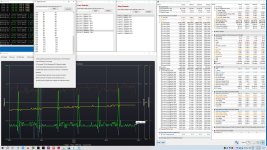
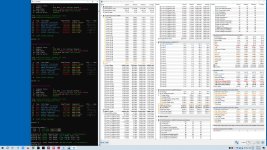
57x, 58x ich soll mit CbR23 testen denke ich, weil SFT boostet nie da. Ganz kurz 720 low Spiel getetsted, boosted locker 59x.
Bonus Video, L0 error, zu wenig Vcore fuer SFT
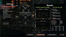
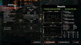
Bonus Bild, TR Benchmark 720 low running. Boosted schoen.
Natuerlich, es ist zu kurz, ich muss laengerer weiter machen/testen, aber ich sehe das Licht in Tunnel
") Keine OC waren. Rebar, HT, HAGS waren an.
Keine OC waren. Rebar, HT, HAGS waren an.Bonus Video, L0 error, zu wenig Vcore fuer SFT
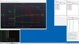
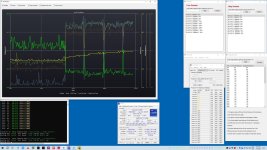
Wait, was this just no curve work 5.7 , or just IA DC 0.01 - causing high effective "fake" clock ?But at same fixed voltage and + "200MHz" fixed more, you compute to nearly the same ~ actually slower.
And if we go clock to clock, quite a bit slower.
@zebra_hun
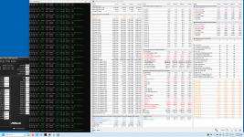
This is V/F Curve. HWINFO shows here. Always it shows the max value.Can you figure me out where this is coming from

Catch curve instability with more programs
And throttle. Like i did~
VT3 is dynamic, but not useful for this sort of tracking.
I made a thinking mistake, because the behavior looked like fixed clock - and the throttle too when i compared load and profilesAnother thing that I don't fully understand when you write that there is no fixed frequency and fixed Vcore.
For my experience, bizarre. Very.This is V/F Curve. HWINFO shows here. Always it shows the max value.
We will see what works.I will do that. All games, lite load, are boosted to 59x, I will only be able to test them with lite load.
What convinced me is that it doesn't boil over, burn, and regulates nicely, even under extremely high loads. Unfortunately, because I see other 14900k cpu's, I need ~100mV extra, so I'll reach the limit sooner. This is what I have, this is what I have to accept.