Du verwendest einen veralteten Browser. Es ist möglich, dass diese oder andere Websites nicht korrekt angezeigt werden. Du solltest ein Upgrade durchführen oder einen alternativen Browser verwenden.
Ahhh,
i feel like i always have to disagree with the whole world , whyy
Ok lets try
OCN people killed their cpu because they dont understand how lapping works (many)
A friend? , collegue killed their CPU because they knocked the SMD element off it while lapping
I lapped my die only a little with 2000 grit, wetted with water. I only took off the top layer in an area about 1 cm square, but in an odd shape due to uneven surface. The uncovered area looks similar to a silhouette in a Rorschach test.
I forgot to take photo after the mild lapping. This sample had very poor adhesion of the solder to the die. The dark areas are the poor adhesion; the solder just flaked off. Meanwhile the lighter areas had solder that was very stubborn to come off and required 3-4 applications of small amount of LM to dissolve/break free.
Zuletzt bearbeitet:
Wenn Du diese Anzeige nicht sehen willst, registriere Dich und/oder logge Dich ein.
I lapped my die only a little with 2000 grit, wetted with water. I only took off the top layer in an area about 1 cm square, but in an odd shape due to uneven surface. The uncovered area looks similar to a silhouette in a Rorschach test.
I forgot to take photo after the mild lapping. This sample had very poor adhesion of the solder to the die. The dark areas are the poor adhesion; the solder just flaked off. Meanwhile the lighter areas had solder that was very stubborn to come off and required 3-4 applications of small amount of LM to dissolve/break free.
Yes, i was educated to use a slightly distilled ferric chloride solution.
Usually you use the normal concentration for etching the top layer on Damascus knifes
Or in our usecase, "we" use it to etch traces into the thin copper layer of the PCB.
On the crystal it doesnt harm it, but dissolves the Indium.
If i'm not mistaken it doesnt touch the passivation layer ~ which does show blue-purple refractions under sunlight.
LM does eat this one away unfortunately.
There are many things i dislike about any Galium mixture, but i understand why its soo widely used.
Its viscose and has a quite high Z axis conductivity, when little amount of if makes contact
// sadly also it has a high thermal transfer resistance, especially on the Z axis ~ compared to something like graphene or even PTM
I do think tho that most (if 3 parts) are not viscose enough to actually fill all cavities
But there are still plenty of benefits for liquid TIM usage on a sub-optimal contact surface (distance).
Unfortunately yes
People usually dont care nor measure.
We are all too afraid to crack the die (with reasaon)
But dont try to understand why the corners crack ~ when everybody thinks that the crystal is flat.
Its not , not at all. But one cant know without a measurement.
The dark gray things may be a chemically messed with (old) passivation layer
Tho indium does stick to it, if a gold layer was deposited via sputtering.
Actually most of the layers, especially interesting in the LED industry ~ are chemically or magnetically deposited on it.
LM does eat it away, but so does lapping too, sadly
I dont think there is a clean way to preserve it, but given you remove it i wouldnt use gallium at all.
As when the crystal is flat enough for ringing to occur - LM is able to permanently fuse to it (as a thin layer)
It will literally bound both materials together and not just deposit itself onto it ~ which some call "dryout"
In the worst case, this will result in chip flaking, because it will chemically solder both materials.
Also unfortunately its not an IF, but a WHEN topic. Nickel does only slightly slow it down.
EDIT:
In our best case and most common case
It just "dries-out" because there is enough of an air gap on users system
For it to turn into a thin oxidation layer without permanently bonding both materials together
// Basically users distance always was high enough, soo this inevitable event doesn't occur in its fullest worst-case
I probably will remain to dislike it, because if you already try to go direct-die
Your first and foremost focus should be a good contact, for lower thermals to occur. // because thermal-transfer-resistance is the most annoying part of any TIM. Plain air has the highest one.
Air is a far too good insulator, and it wouldnt matter much how well thermal transfer resistance is ~ when the Z-Axis is tiny (~50µm), compared to normal usecases of 150-200 microns
There the paste quality wouldnt matter and you'd prefer something with much finer ingredients compared to our common viscose pastes.
Something very liquidy and/or oily that doesnt evaporate.
Ahhh,
i feel like i always have to disagree with the whole world , whyy
Ok lets try
OCN people killed their cpu because they dont understand how lapping works (many)
A friend? , collegue killed their CPU because they knocked the SMD element off it while lapping
I don't want to post or leak private pics, but yes it happens when you do half hearted work on delid (not working with right materials, tho this here was just a normal accident)
Him, he listened to me with Fuji Films.
I guess, excuse me friend Anhang anzeigen 998865
You'll write if you want to be known~
Without lapping you can see how bad it was.
Of course the corners crack first...
All CPUs are at a rollercoaster like igor shows on the pic from the last post Anhang anzeigen 998866
And normal spreading simply wont make it accurate
The issue here is rather the irregular pressure + the sensitivity of the crystal
While the paper needs software to map out the height, it does show it well with PSI how inconsistent it is
This goes to everyone who removes indium with scraping and doesnt dissolve it.
For them its much worse, due to creating micro caveats with their scratching ~ instead using MG415 ferric chlorite to dissolve it.
LM is a liquid TIM
It has decently high viscosity soo "it goes by" fine when you use a bit more
With the tradeoff of high Z axis thermal resistance and chance of insta killing something
Outside that, that it fuses to the surface permanently when we speak about sub 100 microns distance. (chemical fusing to crystal)
The biggest downside is, you need sub 100 microns height difference, to make use of liquid-tim. Any sort
MX-4 is one of those sorts
Its overall a "suboptimal" paste if we compare it to the OC APEX or Kryo/KPX
But they also benefit because of the viscosity.
so called pumpout isnt such an issue anymore with sub 100 microns height difference.
I dont know how "slow" it is
Because i dont know anybody who nails this. Crystal to IHS.
Nobody seems like cares about this and then complain that their ~100+ microns seaboard CPU doesnt make perfect contact with their donut waterblock
I dont know~~
PTM itself is an issue,
because it requires high pressure.
Its great for resolving the common .2mm irregularities and stamp inconsistencies between IHS and Block.
For notebooks it somehow works out well, but i believe its due crystal being thicker and hence surdiier.
Same to GPUs. Much thicker.
I would not trust it to take the required pressure on the bare die.
Especially as this increases drastically the chance of people cracking their corners or bending their substrate like a banana.
Seen both now too often
Nm screw drivers while matter for pressure, do not matter in resolving the left airgaps.
if anything, it would make it suboptimal, because one gap might be hiigher than the other , and so this gap will let the CPU be bent screwed in.
Its unpreventable unless you lap both parts as flat as possible.
And "how flat" can only be measured, not felt
// the lowest you can "test it" with is a grocery store recipe or any very thin paper this is around 100microns thick. +/- 5 to 10µm
Usually those LLLW's sell for 50-60$. the LLLLW for 100-120$
It feels like a no brainer seeing their sample pack for 10$
Beitrag automatisch zusammengeführt:
Here i expect Roman to know better and just missexplained or community quoted wrongly.
What messes with memOC, is having a huge copper plane that will act as ground
Right above the traces.
Energy moves in free space, and may pick a metallic material as travel path (up to frequency if it runs along it "skin effect" or penetrates through it)
Having a huge huge copper blob right above the traces totally will skew with them.
Like its not even a question, but seems unfortunate that Board layer count is not heigh enough to isolate that near/under the socket.
Graphite i dont think has similar properties, and outside that ~ the crystal is many layers
It will not pick the Z axis as travel up path. There are too many layers between it
Else every metallic cooler would cause trouble.
It also can not be due to sheet creating more mounting pressure, as that is maybe 50 -70microns more (its compressable)
Yet Socket springs have leeway on them too. Another reason why some people overtighten their stuff and create a banana CPU
Because they don't understand that the mounting pressure is done by the frame. The waterblock just barely touches the chip.
Roman having a full copper base (around the socket) right above the traces,
Is what caused the issues and why POM was a better decision, or offsetting it higher ~ like he mentioned on the Mycro Dev talk.
Today I teared the O ring on the Supercool block and flooded the RAM slots with ccolant. (wanted to reapply the LM and play with the tightening a little bit.)
My PC decided to not turn onn with RAM in DIMM A, so I cleaned the slots, and the CPU socket and installed my good old Iceman block.
And guess what? It's better. At least my TG Xtreem started to work. It will worth to put the waterblock on it.
I flooded everything, even the dimm.2 slot too. That made the boot hang on 00 for some seconds.. it's removed now, should dry out a little. Gskill works too just this was easier for slot testing without water block.
8400 was never happened on this particular Teamgroup kit.
But I am still looking for answers, acts totally different compared to Gskill. This one doesn't like the high in-mem deltas.
I need some time to find out.
Started on water from 8200C36 to find out how it works.
Cleaned and polished the block and the die, reseated several times. Now the temps are looking okay.
MVDD: 1.48V
MVDDQ: 1.44V
SA: 1.20V
CPUVDDQ: 1.28V
VDD2: 1.431V
RON 48/40 - 40/48 (RON training disabled, VDDQ training disabled)
Did some work on the PC during the test, so bitrate is not constant.
@Veii
Got a new 14900KS and have hard time getting 8000 VST/VT3 stable. I remembered you suggesting to run MC SP x 5 to see how constant are the values. So i did that and got, 80-86-80-84-87. I use a TR contact frame, so this might be the issue? Shall i change to original ILM and retry?
BTW here is my VF table, so im open to voltage suggestions. My 2x16GB kit can run 25 loops TM5 Usmus at 1.47/1.41 8000 36-36-36-58 no issues.
Yes, i was educated to use a slightly distilled ferric chloride solution.
Usually you use the normal concentration for etching the top layer on Damascus knifes
Or in our usecase, "we" use it to etch traces into the thin copper layer of the PCB.
On the crystal it doesnt harm it, but dissolves the Indium.
If i'm not mistaken it doesnt touch the passivation layer ~ which does show blue-purple refractions under sunlight.
LM does eat this one away unfortunately.
There are many things i dislike about any Galium mixture, but i understand why its soo widely used.
Its viscose and has a quite high Z axis conductivity, when little amount of if makes contact
// sadly also it has a high thermal transfer resistance, especially on the Z axis ~ compared to something like graphene or even PTM
I do think tho that most (if 3 parts) are not viscose enough to actually fill all cavities
But there are still plenty of benefits for liquid TIM usage on a sub-optimal contact surface (distance).
Unfortunately yes
People usually dont care nor measure.
We are all too afraid to crack the die (with reasaon)
But dont try to understand why the corners crack ~ when everybody thinks that the crystal is flat.
Its not , not at all. But one cant know without a measurement.
The dark gray things may be a chemically messed with (old) passivation layer
Tho indium does stick to it, if a gold layer was deposited via sputtering.
Actually most of the layers, especially interesting in the LED industry ~ are chemically or magnetically deposited on it.
LM does eat it away, but so does lapping too, sadly
I dont think there is a clean way to preserve it, but given you remove it i wouldnt use gallium at all.
As when the crystal is flat enough for ringing to occur - LM is able to permanently fuse to it (as a thin layer)
It will literally bound both materials together and not just deposit itself onto it ~ which some call "dryout"
In the worst case, this will result in chip flaking, because it will chemically solder both materials.
Also unfortunately its not an IF, but a WHEN topic. Nickel does only slightly slow it down.
EDIT:
In our best case and most common case
It just "dries-out" because there is enough of an air gap on users system
For it to turn into a thin oxidation layer without permanently bonding both materials together
// Basically users distance always was high enough, soo this inevitable event doesn't occur in its fullest worst-case
I probably will remain to dislike it, because if you already try to go direct-die
Your first and foremost focus should be a good contact, for lower thermals to occur. // because thermal-transfer-resistance is the most annoying part of any TIM. Plain air has the highest one.
Air is a far too good insulator, and it wouldnt matter much how well thermal transfer resistance is ~ when the Z-Axis is tiny (~50µm), compared to normal usecases of 150-200 microns
There the paste quality wouldnt matter and you'd prefer something with much finer ingredients compared to our common viscose pastes.
Something very liquidy and/or oily that doesnt evaporate.
I also have a 0.3mm Z-axis height chemical vapor deposition diamond heatsink that I haven't tried. I paid a company in China to manufacture it.
Even though the Z-axis thermal conductivity is supposed to be very high (1400 W/mK) it still adds Z-axis height for the heat to move through to get to the water if placed between direct die coldplate and die, so I lately I don't think it will improve things. It adds a bit of thermal mass (25mm x 13mm x 0.3mm=0.0925cm^3, 3.51g/cm^3 x .0975cm^3= 0.342g).
It may also help move heat in x and y axis a bit to be accepted by a larger area of the coldplate. It has advertised horizontal thermal conductivity of 600-700 W/mK.
I have dreams of designing a direct die block with only CVD diamond between the water and the TIM to the die. The diamond for this application would need to be much larger than the one I have as it is only slightly larger than the dimensions of the die and would cost something like $500 US just for the diamond portion.
EDIT: If chemical bonding between the LM and the die is to be worried about, perhaps my diamond heatsink would be a good permanent fixture to a fully lapped die. I wonder if thermal transfer would be the same once the chemical reaction is fully complete and all the LM is bonded to the crystal? It is a good CPU sample and I wouldn't mind this happening if thermals are good.
With meteor forged chemically deposited layer or unicorn sparkles blessed by the poope.
Too many buzz words
Basically a copper heatsink with (or allu), idk what that last part is supposed to mean
Got any pics of that thing
Given the need of buzz words, i would doublecheck its manufacturing tolerances, because ya
Too much marketing, too little data for the product to speak about itself
EDIT:
I understood later nvm
But your problem still will be the layer created to your waterblock. Nickel will not prevent it, just slow it down
Even though the Z-axis thermal conductivity is supposed to be very high (1400 W/mK) it still adds Z-axis height for the heat to move through to get to the water if placed between direct die coldplate and die, so I lately I don't think it will improve things. It adds a bit of thermal mass (25mm x 13mm x 0.3mm=0.0925cm^3, 3.51g/cm^3 x .0975cm^3= 0.342g).
If copper, its the same thing
Thermal conductivity rating is such a marketing word
Material thermal-transfer resistance is what plays a key role ~ as its the factor of when wm/k even starts to matter.
Same one goes for direct-die shenanigans.
You only need a heatsink if the gap is big, mostly past 200 microns where pads come into play as liquid TIM loses usefulness on such a gap.
Its difficult.
Cant trust the manufacture getting their tolerances low.
Cant trust to begin with that they have the proper measuring equipment like only two of our reviewers in the EU (der8auer and igorslab)
I mean, even Roman struggles with manufacturing tolerances here and there, imagine a small company making 3rd party IHS ~ nvm
I have dreams of designing a direct die block with only CVD diamond between the water and the TIM to the die. The diamond for this application would need to be much larger than the one I have as it is only slightly larger than the dimensions of the die and would cost something like $500 US just for the diamond portion.
Probably would recommend to invest resources into graphene stuff
its less the material or the indium thats the "issue".
Its the gaps and lack of flatness which brings people to go the delid route - just to mess up again and introduce airgaps 🤭
Ah, nothing good can come out of this talk haha.
I wish finer work soo one can be an exemplary person for everyone else. But i dont know. Still waiting for this day to happen;
Ah vaporchambers are nice too, but all is just a bandaid to fix user introduced issues ~ aka airgaps
With positive benefits i guess, to prevent the crystal from cracking. And some thermal expansion factors i dont fully get (see Der8auers Intel-HQ interview video about delids)
EDIT: If chemical bonding between the LM and the die is to be worried about, perhaps my diamond heatsink would be a good permanent fixture to a fully lapped die.
Its galium that is ... annoying
Because the bonding, in this case chemical fusing is unpreventable
In the best case its a low factor because a waterblock or aio doesnt vibrate much
soo unless you one shot it and trust (never remove it) , it doesnt matter if it fuses
sputtering is a really cool tech
But all that is soo overkill
One has to also think how to protect the pcb from that ~ and especially the bottom side of the CPU, or the airgaps left behind between the die-> substrate layer
// thick coating around the edge of the crystal
Soo much work invested, for such a little issue ~ user error
Just get the gap tiny or at very least flat , and use a liquid TIM that will not evaporate till 140°C. All issues resolve
Material ringing is a very interesting property and barely understood tlll today.
usually a droplet of machine-oil is plenty to hold both together, if there wasnt only the thermal expanding factor
Eh the crystal is stable enough between -100 -> 200°C.
Only your waterblock should be your worry and the roomtemp flatness of the crystal.
TIM Wm/K is very little relevant.
(Wm/K layer * material thermal-conductivity on Z-Axis , div by psi & tensile strength . , Times or divided by something called thermal transfer resistance ~ not the same as Z-Axis W/mK.) // very novice on this topic
// Basically users distance always was high enough, soo this inevitable event doesn't occur in its fullest worst-case
Thermal transfer resistance, only matters up to how much user error (airgap) you leave behind *
I would completely skip gallium mixtures on the good outcome - because it will fuse and any removal = diecrack.
* see Roman's inspiration for Z-Axis oriented Graphite Pad
// which did do a bit but not too much as its still 200 microns thick and likely deformable down to 120microns (a guess)
// probably still a much better option against user error than using high pressure on PTM ~ on a bare crystal
EDIT2:
Fuse instead Dryout ~ because dryout mostly happens due to leaving airgaps behind.
A blob who's outer layer chemically reacts with air and dries out, should form a vacuum seal to the rest of the material. // till block-vibrations break/disassembly breaks that
As the chance is too little that air is inside the gallium blob for it to fuse on the center.
What is more common and keeps on happening, is the blob only being bound to Cooler by surface tension - never by the flatness of both materials.
// which is also "surface tension" 🤭 but you get my point .
LM is not a very liquidly material.
EDIT:
In our best case and most common case
It just "dries-out" because there is enough of an air gap on users system
For it to turn into a thin oxidation layer without permanently bonding both materials together.
But I am still looking for answers, acts totally different compared to Gskill. This one doesn't like the high in-mem deltas.
I need some time to find out.
RTTs
G.Skill uses own stuff.
Teamgroup & OloY , mutually most likely use a similar thing
Chance is very high to be the "common" HJ 10 Layer.
its a bad timing ~ but it would be good to use the G.Skill's and find your old base again with manual RTTs.
Then we can transfer this to the Global HJ's.
I'm just used to stuff that follows specifications and is predictive in its behavior // well not only
Your old base was 8533 right ?
Wanna spend time on it for the TG Xtr ?
Would be useful time for the public ~ tho it still will be "your APEX" related
I actually would also like to try and cut VR MAX down to 1500mV @ 400A ICCMAX
Last days calculations makes it fit just perfectly inside 400A.
I would like to know if i understood VID spreading well, or UncoreVID will cause me/us trouble.
If you find the time, can you make me a table/paper writing with the ~score~ results on:
GB3 (Core+Mem), GB6, CB23 or 24, CB15 Extr, y-cruncher FFT 3-4 loops (takes 8min max)
Between 1600mV and 1500mV VR MAX.
^ it may destabilize your memOC ~ but probably first result in degraded boosting perf
Happy to see Intel finally "coincidentally" agreed on 400A as absolute max.
nice to seee ~ tho they remain silly with PT1 = PT2 ideology.
Now they just need to agree at 1600mV VR MAX vs 1720 and remake the basic curve through ME update.
Then we are golden and i'm happy with my talk against a brickwall~~
@Veii
Got a new 14900KS and have hard time getting 8000 VST/VT3 stable. I remembered you suggesting to run MC SP x 5 to see how constant are the values. So i did that and got, 80-86-80-84-87. I use a TR contact frame, so this might be the issue? Shall i change to original ILM and retry?
Whoever makes the frame is not as important as your own caused mistake
Yea please remount
TR frame can be tightened down nearly fully ~ but if you apply too much pressure by your cooler, you'll mess it up
Pressure only needs to come from the frame.
TR screws sadly loose grip over time
They are cheap. I broke them twice so far
I would suggest on an Apex to see if its flat on the original mount + original screws (put the protective cover on)
And if not, loose all backside screws a bit, so we dont have a banana Board.
Only then tighten down your Socket mount. Dont do the reserve order please.
Its a comment link ~ test
Sadly YT is silly and this + marked comment, will neither reach Jay nor Falcon Northwest's suggestion ~ which had some issues
If community wants to bother and rate this up or upload/send it to them
YT Part1 + screenshot Part2
It would help the community~
@Darkthrone , use ASUS Tool.exe to manipulate your V/F curve.
Do not use Telemetry Faking.
Whoever makes the frame is not as important as your own caused mistake
Yea please remount
TR frame can be tightened down nearly fully ~ but if you apply too much pressure by your cooler, you'll mess it up
Pressure only needs to come from the frame.
TR screws sadly loose grip over time
They are cheap. I broke them twice so far
I would suggest on an Apex to see if its flat on the original mount + original screws (put the protective cover on)
And if not, loose all backside screws a bit, so we dont have a banana Board.
Only then tighten down your Socket mount. Dont do the reserve order please.
Sadly the Apex is in the case and cant check if its any wrapped or not.
I use an Alphacool Core 1 cpu block + backplate. Shall i tighen the TR frame at the max, and block + backplate go by hand till it start to get resistance? Does this sound good?
Btw TR frame uses the boards ILM screws, does not have any in the box.
I use an Alphacool Core 1 cpu block + backplate. Shall i tighen the TR frame at the max, and block + backplate go by hand till it start to get resistance? Does this sound good?
Btw TR frame uses the boards ILM screws, does not have any in the box.
Oh thats funny
Guess its a good thing, because they were bad and breaking inside the Backplate
Only your drill saved you then.
Yes, does the Alphacool core Manual not say "tighten fingertight" ?
My suggestion is, to hold thumbscrews with first 3 fingers (tingertipps) and then tighten as strong as you can be ~ but only use the fingertipps.
Thats plenty and around .6Nm . Tho Nm "depends"
Alternative is to full tighten and then unscrew all 4 screws a bit, but that gives a random variable.
I remember my Alphacool mount does have springs and washers
The springs are hard to put in, so i had to use a screwdriver just to press them into the backplate
Then fingertips-tight only
Can force to 1.1ohm
between 1.08-1.12 or so ~ Boardloss focused. Usually LCC also should stay droopy , because its either LLC or its IA_LL messing.
// i can do both because i do silly stuff sometimes - but dont do as me. Do it right. Messing with LLC is also quite suboptimal as you never have measured the Board.
// Boardpartner knows the best the required LLC of their designed Board
Intel is also doing mystery work and jumps between 1.1ohm and 1.7ohm , haha.
They can't decide on something and neither does ME reflect it. Till recently it was 0.5ohm with a high high voltage default curve that can supply 1.7v to the CPU when 2 cores are loaded.
Oh dear.
PL1/2 limiters should be only your worry with an AIO or a weak PSU.
They are dynamic slow limiters and do not matter if they are high or inf. They should have some logic in them tho, aka PL2 be what its supposed to be, a short boost limiter.
If they are tight, you will throttle on many places ~ which factors in your memoryOC voltages too.
With VR MAX of 1600mV , you also will mess with the curve,
because all by default is far too overvolted.
I suggest to work on your curve, and lower it ~ else you may not come far with memOC ~ as you'll reach CEP and other throttle points by stock operation
// that's how bad it is right now, well always was.
At least its safe,
But it will be throttle hell till you fix curve yourself.
Als Spaß habe ich "Intel Dreams" 56x allcore, 60x 2 core Profil gebaut.
Mit meinem CPU ist es ünmöglich einpacken ins Intel Baseline.
CEP muss aus, Amper Grenze auch, sonst throttle.
Ich glaube habe ich gute Kurve gemacht, IA AC LL 0.48, so ist die Vcore 1.17V und VID 1.18V.
Mir ist egal, ich will überhaupt nicht 56x sehen und nutzen, nun wollte ich dieses Frequenz sehen.
Kein throttle is, Werte sind richtig gut meine ich.
Ja, ~280 Watt.
Ich kann es "cheaten", DC LL runter, Hwinfo VID zeigt weniger, und rechnet weniger Watt.
Ich wollte es nicht, DC auf auto geblieben.
+0.01V zu Vcore glaube ich normal und richtig.
90 min Misch ohne Problem durcgelaufen ist.
1.16V reicht, aber wie wir letztes mal gesehen haben, Cb R15 Extreme braucht mehr Vcore. Deswegen habe ich bischen mehr gegeben.
Wie gesagt hab, nur für Spaß, 56x ist zu viel.
Ich bin sicher, dass es für Alltags macht kein schlechtes, wer will, kann so lassen.
Nur Y Cruncher "kostet" 280W, Games 60-80W.
54x in Games 50-70W.
Vcore Latch max 1.43V war.
Oh thats funny
Guess its a good thing, because they were bad and breaking inside the Backplate
Only your drill saved you then.
Yes, does the Alphacool core Manual not say "tighten fingertight" ?
My suggestion is, to hold thumbscrews with first 3 fingers (tingertipps) and then tighten as strong as you can be ~ but only use the fingertipps.
Thats plenty and around .6Nm . Tho Nm "depends"
Alternative is to full tighten and then unscrew all 4 screws a bit, but that gives a random variable.
I remember my Alphacool mount does have springs and washers
The springs are hard to put in, so i had to use a screwdriver just to press them into the backplate
Then fingertips-tight only (and)
Can force to 1.1ohm
between 1.08-1.12 or so ~ Boardloss focused. Usually LCC also should stay droopy , because its either LLC or its IA_LL messing.
// i can do both because i do silly stuff sometimes - but dont do as me. Do it right. Messing with LLC is also quite suboptimal as you never have measured the Board.
// Boardpartner knows the best the required LLC of their designed Board
Intel is also doing mystery work and jumps between 1.1ohm and 1.7ohm , haha.
They can't decide on something and neither does ME reflect it. Till recently it was 0.5ohm with a high high voltage default curve that can supply 1.7v to the CPU when 2 cores are loaded.
Oh dear.
PL1/2 limiters should be only your worry with an AIO or a weak PSU.
They are dynamic slow limiters and do not matter if they are high or inf. They should have some logic in them tho, aka PL2 be what its supposed to be, a short boost limiter.
If they are tight, you will throttle on many places ~ which factors in your memoryOC voltages too.
With VR MAX of 1600mV , you also will mess with the curve,
because all by default is far too overvolted.
I suggest to work on your curve, and lower it ~ else you may not come far with memOC ~ as you'll reach CEP and other throttle points by stock operation
// that's how bad it is right now, well always was.
At least its safe,
But it will be throttle hell till you fix curve yourself.
So i can keep LLC 5 and just have AC LL/DC LL at auto?
I want to keep PL1/PL2 as low as possible to prevent any kind of degradation till i have my mem tuned. Thats why i keep both Pcores low and set PLs
With VR MAX of 1600mV , you also will mess with the curve - So which vlaue is ok?
I suggest to work on your curve, and lower it/But it will be throttle hell till you fix curve yourself. - From the OC tool where can i find the VF curve so i can post it here for some advice?
With meteor forged chemically deposited layer or unicorn sparkles blessed by the poope.
Too many buzz words
Basically a copper heatsink with (or allu), idk what that last part is supposed to mean
Got any pics of that thing
Given the need of buzz words, i would doublecheck its manufacturing tolerances, because ya
Too much marketing, too little data for the product to speak about itself
EDIT:
I understood later nvm
But your problem still will be the layer created to your waterblock. Nickel will not prevent it, just slow it down
If copper, its the same thing
Thermal conductivity rating is such a marketing word
Material thermal-transfer resistance is what plays a key role ~ as its the factor of when wm/k even starts to matter.
Same one goes for direct-die shenanigans.
You only need a heatsink if the gap is big, mostly past 200 microns where pads come into play as liquid TIM loses usefulness on such a gap.
Its difficult.
Cant trust the manufacture getting their tolerances low.
Cant trust to begin with that they have the proper measuring equipment like only two of our reviewers in the EU (der8auer and igorslab)
I mean, even Roman struggles with manufacturing tolerances here and there, imagine a small company making 3rd party IHS ~ nvm
Probably would recommend to invest resources into graphene stuff
its less the material or the indium thats the "issue".
Its the gaps and lack of flatness which brings people to go the delid route - just to mess up again and introduce airgaps 🤭
Ah, nothing good can come out of this talk haha.
I wish finer work soo one can be an exemplary person for everyone else. But i dont know. Still waiting for this day to happen;
Ah vaporchambers are nice too, but all is just a bandaid to fix user introduced issues ~ aka airgaps
With positive benefits i guess, to prevent the crystal from cracking. And some thermal expansion factors i dont fully get (see Der8auers Intel-HQ interview video about delids)
Its galium that is ... annoying
Because the bonding, in this case chemical fusing is unpreventable
In the best case its a low factor because a waterblock or aio doesnt vibrate much
soo unless you one shot it and trust (never remove it) , it doesnt matter if it fuses
sputtering is a really cool tech
But all that is soo overkill
One has to also think how to protect the pcb from that ~ and especially the bottom side of the CPU, or the airgaps left behind between the die-> substrate layer
// thick coating around the edge of the crystal
Soo much work invested, for such a little issue ~ user error
Just get the gap tiny or at very least flat , and use a liquid TIM that will not evaporate till 140°C. All issues resolve
Material ringing is a very interesting property and barely understood tlll today.
usually a droplet of machine-oil is plenty to hold both together, if there wasnt only the thermal expanding factor
Eh the crystal is stable enough between -100 -> 200°C.
Only your waterblock should be your worry and the roomtemp flatness of the crystal.
TIM Wm/K is very little relevant.
(Wm/K layer * material thermal-conductivity on Z-Axis , div by psi & tensile strength . , Times or divided by something called thermal transfer resistance ~ not the same as Z-Axis W/mK.) // very novice on this topic
// Basically users distance always was high enough, soo this inevitable event doesn't occur in its fullest worst-case
Thermal transfer resistance, only matters up to how much user error (airgap) you leave behind *
I would completely skip gallium mixtures on the good outcome - because it will fuse and any removal = diecrack.
* see Roman's inspiration for Z-Axis oriented Graphite Pad
// which did do a bit but not too much as its still 200 microns thick and likely deformable down to 120microns (a guess)
// probably still a much better option against user error than using high pressure on PTM ~ on a bare crystal
EDIT2:
Fuse instead Dryout ~ because dryout mostly happens due to leaving airgaps behind.
A blob who's outer layer chemically reacts with air and dries out, should form a vacuum seal to the rest of the material. // till block-vibrations break/disassembly breaks that
As the chance is too little that air is inside the gallium blob for it to fuse on the center.
What is more common and keeps on happening, is the blob only being bound to Cooler by surface tension - never by the flatness of both materials.
// which is also "surface tension" 🤭 but you get my point .
LM is not a very liquidly material.
I'll send photo today after I return home from work of my diamond heatsink.
It isn't a product. I contracted a manufacturer in China to make it per my specifications (dimensions).
The salesman has been hounding me for 8 months asking what the performance is like. I still haven't installed it
EDIT: Chemical Vapor Deposition is the name of the manufacturing process, not buzzwords. They bombard the surface with carbon atoms in gas form to crystallize on a substrate in a specific environment (temperature, pressure, etc). This is purely an idea I had that may help get the heat out of the die more quickly, and spread over a larger surface area that makes the contact area with the coldplate larger.
Chance is very high to be the "common" HJ 10 Layer.
its a bad timing ~ but it would be good to use the G.Skill's and find your old base again with manual RTTs.
I think I was walling with the Gskills. Now I am not even close to that, but working on it.
I will order the Der8auer block, hope the MC will be more consistent with that.
Maybe my Encore is the wall. Not sure about that.
I actually would also like to try and cut VR MAX down to 1500mV @ 400A ICCMAX
Last days calculations makes it fit just perfectly inside 400A.
I would like to know if i understood VID spreading well, or UncoreVID will cause me/us trouble.
If you find the time, can you make me a table/paper writing with the ~score~ results on:
GB3 (Core+Mem), GB6, CB23 or 24, CB15 Extr, y-cruncher FFT 3-4 loops (takes 8min max)
If you force low clock and force IVR to throttle mem voltage
What are you working on to test ?
Wattage is average powerdraw metric
You can run them as:
PL1/2 is not soo relevant
Pic is updated those values are better, but non of those causes degradation haha.
It will hit ICCMAX first. PL1/2 are not degradation limiters. Rather powersupply protectors
They are average thermal limiters. Way to slow to be used as current limiters.
EDIT: Chemical Vapor Deposition is the name of the manufacturing process, not buzzwords. They bombard the surface with carbon atoms in gas form to crystallize on a substrate in a specific environment (temperature, pressure, etc).
Yes there is an edit at the very first quote with "nvm i understood , its not a random manufacture"
CVD, they call sputtering too. mhm mhm - i'm aware
Unfortunately even that process is far from flat.
You need to start from a flat surface, else lapping that layer will cause you much trouble.
Lets see the outcome
Curious about 3 things
substrate to crystal height
crystal to IHS height
And if you have factored in the additive height of the corner feet (silicone glue)
Unless you thought to do that on the native IHS ?
Still not entirely sure
Curious about 3 things
substrate to crystal height
crystal to IHS height
And if you have factored in the additive height of the corner feet (silicone glue)
Unless you thought to do that on the native IHS ?
Still not entirely sure
mmmm if you've considered to make something like the Mycro
Please reconsider to surround the chip with a conductive material, near the traces.
It needs a bit of distance and an insulator or just a material with as little as possible conductive properties.
// to be more clear, a material which has low capacitance. Close to zero. Air is such one
A huge blob of copper (like a cage around the socket, or right above the PCB) will completely ruin your transmission lines.
And a material with dielectric properties may mess with it. Need an insulator if right above the magnetic fields of the transmission lines.
EDIT:
If you put a huge blob of copper around it, it will act as a Ground and leech magnetic energie to it, instead of letting it run along the transmission lines.
Like if you touch a live wire, you have a high chance to become the path of least resistance.
Magnetic fields love to travel in the Z axis , vs along the X or Y axis. PCB layers are stacked on the Z-Axis.
I wonder how much you removed
100 microns you can remove from the crystal.
150 becomes dangerous already
200 i can not recommend anymore.
mmmm if you've considered to make something like the Mycro
Please reconsider to surround the chip with a conductive material, near the traces.
It needs a bit of distance and an insulator or just a material with as little as possible conductive properties.
// to be more clear, a material which has low capacitance. Close to zero. Air is such one
A huge blob of copper (like a cage around the socket, or right above the PCB) will completely ruin your transmission lines.
And a material with dielectric properties may mess with it. Need an insulator if right above the magnetic fields of the transmission lines.
EDIT:
If you put a huge blob of copper around it, it will act as a Ground and leech magnetic energie to it, instead of letting it run along the transmission lines.
Like if you touch a live wire, you have a high chance to become the path of least resistance.
Magnetic fields love to travel in the Z axis , vs along the X or Y axis. PCB layers are stacked on the Z-Axis.
I can't imagine I removed even 100 microns yet. Maybe 50. Only a small area in the center of the die is missing the outer layer. Maybe 1 cm^2.
There will be no additional conductive/inductive material. Only 13x25x0.3mm diamond heatsink (die is ~12mm x 23mm). Just Supercool direct die coldplate and that is it. It is same dimensions as IHS.
If you force low clock and force IVR to throttle mem voltage
What are you working on to test ?
Wattage is average powerdraw metric
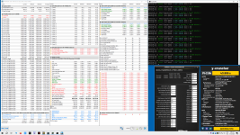
You can run them as: Anhang anzeigen 999640 PL1/2 is not soo relevant
Pic is updated those values are better, but non of those causes degradation haha.
It will hit ICCMAX first. PL1/2 are not degradation limiters. Rather powersupply protectors
They are average thermal limiters. Way to slow to be used as current limiters.
I am testing VST/VT3 for mem stability.
So i changed PL1 256w/PL2 320w/ICC MAX 400A/IA VR MAX 1600mv/AC LL Auto
Now Cine23 run at 56/44/44 1.172v-1.181v 253w and VST at 55/44/44 1.163-1.172 270w which is far more than it needs.
Which option shall i use in OCTool to link you the VF curve?
I will try that later. At friday I ran almost 3 hours of Y on 8400C36, then I rebooted and got error 53 Qcode. Couldn't even boot.
So started to troubleshoot with the typical things. Tried different memories, reseated the CPU several times, CMOS battery removing, different dimm slots, BIOS flashback...etc...
None of them helped.
So I tought maybe I still have some coolant in my dimm slots. What I can't clean out with ordinary tools, so took my 8 bar compressor and airgun and cleaned every socket with air pressure. And it booted.
But now I have stability issues again, so started to troubleshoot. Seriously, it really annoys me now, but it's my fault, pushing too hard.
This KS is so hard to reseat correctly. I believe it should have something with the die height. It was already polished when I got it. Maybe too thin?
The higher the pressure is the higher MC SP for me, which is strange.
My KF just worked, no matter what, that was polished by me.
I have some 1000 grit sandpaper here, I wonder should I check the die with a liner and try to polish it. What do you think? Maybe that would help with the MC SP fluctuation as you suggested before.
Man kann durch schleifen des "Die" den IMC verbessern? Geht der Mem dann höher, oder nur der wie es heißt falsche Wert im Bios?
Wäre es nicht einfacher, sich einfach eine bessere CPU zu kaufen?
Can you improve the IMC by grinding the "Die"? Does the Mem then go up, or is it just the wrong value in the BIOS?
Wouldn't it be easier to just buy a better CPU?
I can't play the lottery, I buy the parts as a companny, can't just send it back if I don't like it. ☺️
It's not a bad CPU at all, max stable is 8533, same as my KF.
I would buy prebinned CPU, but no one can give me invoice from that. 🤣
Es gibt noch eine Option. Kaufen, testen und auf dem Gebrauchtmarkt verkaufen.
Nachdem ich ein paar Tage im OCN unterwegs war, frage ich mich, wieso ihr euch nicht dort austauscht. Das, was ihr hier in englisch ausbreitet, ist dort den ganzen Tag Thema, habe ich das Gefühl. Diese ganzen Loadline/Köpfen/Kühler Geschichten haben doch recht wenig mit Mem OC zu tun. Passt doch eher in ein Wakü Thread oder OCN Intel OC Thread.
Got confused
Indium should have been between 250-350 microns (0.25-0.35mm)
Well ~200 + silicon feets/ring of IHS.
Its a far too small range to measure unless you invest in mitutoyo measuring gear with a ruby ball (not worth for your task)
I wonder if those acrylic lapping supports still exist for LGA1700 chips. They had fine steps on them.
Interesting.
Well a diamond-crystal cant expand for sure.
Just to understand fully, this is:
~ a single crystaline synthetic grown crystal, like they use for LEDs
~ a copper ? sheet just with a diamond coating deposited on it
~ some other base material that you inspected to have good Z-Axis Wm/K rating, and hopefully low thermal transfer resistance.
I'm sorry, but i didnt write the tool. I dont remember its dropdown position.
By the time you waited for the answer - you could look up how to use it and find the pages
There is no tutorial for it written out.
The curve parts probably sit near the Intel dropdown menu.
Take a look and you will find them. Explore the tool
The "tutorial" of it may lie back ~150 to now ~180 pages back
or if you track mine, zebra's , tibcsi's posts you will also find pictures.
I don't know
Repeat it like couple posts ago how to use it.
Play with it, its straight forward & explore this thread.
You may find answers for other duplicate questions you have~
so took my 8 bar compressor and airgun and cleaned every socket with air pressure. And it booted.
But now I have stability issues again, so started to troubleshoot. Seriously, it really annoys me now, but it's my fault, pushing too hard.
The Blocks, i dont know
The pushing hard in perfection or lowering voltages, or buying stuff you dont need
~ although later part who knows might rule out some things for you
Non of those would be a waste.
Making an accident, oh well stuff happens.
Eh, at worst not flat but tilted. Things you can measure, as waterblocks/aircoolers generally dont tilt easily.
But besides that, i dont think so.
Too thin would crack or make the lithography visible. Hope i used the right word
Basically would clearly show the inner life, haha.
There is space above it, but too low and things crack too easy.
I have some 1000 grit sandpaper here, I wonder should I check the die with a liner and try to polish it. What do you think? Maybe that would help with the MC SP fluctuation as you suggested before.
1000 grit is too little for crystal polishing. You'll just scratch it deeply
1000-1200, even 1600 is for metal polishing. Copper for example or nickel.
2000 may be for steel bars or other material you want shiny , like kettles. EDIT: (not all kettles are soft brass)
2000 should be the bare minimum for the crystal.
// XOCer like bisobiso for GPUs for example use flat knife polishing stones for this type of work. Else a Marble/Glas surface and high grit plus water droplets is the way to go (of course leveling required)
Sure you can start with 1000, but why even scratch it more than needed
Would only use that if i didnt know how to remove indium better.
I can believe MC SP calculations (changes) may happen by a colder state (0°C vs 20°C roomtemp)
I can not believe it has any sort of duration (the testing) for thermals to matter, soo contact thermal transfer wouldnt be such a big issue
Only uneven pressure would be. But too much pressure on socket also is not too forgiving in the long term. Those are springs after all.
Yet also, thats a far too low chance, given all are factored in when manufacturing as usage and wear tollerances.


")

")