[Sammelthread] Netburst Evolution - Pentium IV/M 478/479 & Xeon 603/604 Stammtisch

Thank you for the clarification! I will add this to my post.
When I did the tests with the ASUS board, I saw, that both settings are unclear or wrong. I wasn't able to figure it out.
I still have the Gigabyte board. Someday I want to test this board if it is good for OC and if it differs from AMI BIOS ASUS board. I need a new BIOS chip for it first though.


edit. is this part correct?
Code:
Burst length
   Register b0d6f0 54h [19:16]
       1111 = disable (8 Clocks)
       0000 = enable (4 Clocks)
 
Zuletzt bearbeitet:
Wenn Du diese Anzeige nicht sehen willst, registriere Dich und/oder logge Dich ein.
edit. is this part correct?
Code:
Burst length
   Register b0d6f0 54h [19:16]
       1111 = disable (8 Clocks)
       0000 = enable (4 Clocks)
I can't say about BL right know - my Asus board shows all registers the same for 4 and 8 clocks BL. Maybe it doesn't work or something else. I was referring only to Bus parking. Gigabyte is the only board that has Bus parking and Dynamic page mode, that's why I played with it today.
 
O.K. I've figured out the Burst length.
MCHBar Register 60

bit 4 Burst length
0 - 4
1 - 8

As you know from the definition of BL, for dual channel it's always 4 clocks but for single channel it can be 4 or 8 clocks.
On my setup i865PE, P4 3.0E, 1*512MB BH-5 2-2-2-5 it's been as follows in AIDA64:

3192/3160/3150/107.2 BL8
3175/3136/3150/107.2 BL4

As you can see R/W is a bit higher with BL8. Unfortunately, it can't be changed on-the-fly so if the BIOS has problems setting it correctly (as I believe my Asus P4C800-E BIOS is), then the only thing is to mod the BIOS.
But for dual channel operation which is more common, it doesn't make any difference.

1704633185014.png


BL4 on the right, BL8 on the left.
P.S. now I see that Asus sets BL8 even when BIOS is set to BL4.
P.P.S. I've double checked and it works on Asus as well as defined by Intel - BL=4 for dual-channel mode (despite setting in BIOS) and BL=4/8 for single-channel mode. Previously I've been testing only DC, my mistake.
 
Zuletzt bearbeitet:
Ah, this is nice! I will add it to the list. Many thanks!
I guess it is not that important to us since we use dual channel most, but who knows....

edit. It fills a gap. nice
1704634299960.png
 
I've confirmed BL on Asus boards (read P.P.S. in my previous post).

Also I've played with Winbonds. As we know, normal Winbond chips work at 250MHz with moderate volts like 3.4V. But most sticks didn't work on 865/875.
Long story short - you need tRFC=5.
Asus boards set tRFC4 when CAS=2.0 and tRFC=5 when CAS=2.5/3.0.
So you need to boot with CAS=2.0 @~230FSB, set tRFC=5 via Memset and then you can go higher. Much higher.
Corsair 3500C2 stick @ 3.9V (at idle) via OCZ RAMbooster.

3.9V PAT Corsair C2.png


Unfortunately, for dual channel seems like it's limited by chipset. Only 256MHz so far. The only thing that helps is setting CL=2.5 which is undesirable. Still these seem to be one of the highest Winbond clocks on 865/875.

snaphsot0007.png
 
Nice G1 CPU! Nice finding also! So in theory we could add a option rom that sets the tRFC = 5 setting during boot? To get higher Cl2 clocks?
Maybe the Dual Channel limitation is also limited by a setting?
 
It's a pretty regular G1. I have a bit more than 10 of them, all POST around 300, the very bad ones make 282-293. But they're nice since they are cool and clock good. Although, on TCCD I am limited by them. Maybe need to put them on water.
So in theory we could add a option rom that sets the tRFC = 5 setting during boot?
In theory - yes. But as you understand if we make just an OpROM, it'll set tRFC5 at the end so we won't be able to boot higher than we can now. So we need to make it an early mod or (best) to mod the CAS programming routine. And I still can't find a way to find CMOS programming routines.

Maybe the Dual Channel limitation is also limited by a setting?
Yes, this came to my mind too. But as you can see before, TCCD at 2,5-4-4-8 have no problems working in dual channel up to 295 (CPU limited, maybe more). I thought, tRAS or other major timings could help but seems only CAS helps. And not too far. Maybe we'll find an answer to this but so far it's an open question. Just shared my progress with you.
 
Best I’ve been able to run DC 1:1 so far was 260 using Ultra-X that would do 270+ on NF4. But that was only after setting switching frequency using Ample-X epower.
I might revisit 478 later so will definitely test tRFC5 as well but I’m pretty sure I already tried all major memset parameters for that 260MHz run.
 
Isn't tRFC 5 quite low? Or is this some special setting on intel? Usually you run as low as tRC 7-9 and tRFC 9-12 but not lower on socket 939. On socket 462 it's even higher with a stock value of tRC 13 and tRFC 15...

Also the read/write and write/read turnaround times look quite high, but i also suspect this is "Intel special" and not comparable to A64...

So we need to make it an early mod or (best) to mod the CAS programming routine. And I still can't find a way to find CMOS programming routines.
Same. This is one of the things i'd like to understand on Award 6.00PG. The usual approach by the bios routine is to initialize the chipset with default values (iirc it's called "early chipset init"), perform several checks and then set the correct clocks and timings at a later stage. I've not been able to find that later stage (yet), let alone the code which loads and applies the strap/romsip timings in general.

I believe at least on nforce 2 the BPL (NVDAMC or NVMM) does it, as it even has a special table for certain ram modules. That's why i want to reverse engineer that piece of code. Also DFI found a way to apply alpha timings as a separate option, which other NF2 boards don't. so comparing the different bios might be a good idea. DFI hasn't modified the BPL, but applies it somewhere else. I suspect they hooked some routine and hacked their timings code into the bios.

I mean, you could for example inject custom code into the POST code jump table (link to HWBOT) if it is late enough during the boot process. And even if you need a later injection, you should be able to replace basically any jump instruction, store all register, apply custom code, restore and jump back into to the stock code. Iirc pinczakko described both possibilities in his ninjutsu book.
 
Zuletzt bearbeitet:
Best I’ve been able to run DC 1:1 so far was 260 using Ultra-X that would do 270+ on NF4.
2*512MB 2-2-2-5? Very nice.
Isn't tRFC 5 quite low?
Yes, but the only board that has tRFC description is Abit and I think Memset took it from there. For example in i845 chipsets tRFC goes from 5-11. So maybe in fact 5 is 11 and 1 is 7 for example. Don't look at actual value, think about the bits. We'll probably never know for sure.
 
Wenn man denkt, man hat hier schon alles gesehen… kommt ein noch Verrückterer daher. :oops:

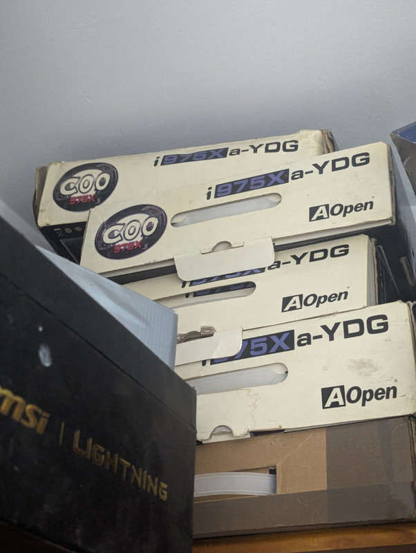
Und wow, so ein 975Xa-YDG hatte ich vor ~ 18 Jahren mal und suche seit inzwischen 5-6 Jahren wieder so eins - ohne Erfolg. Kein Wunder, wenn die alle bei Dir sind.
 
Has anyone seen something like this on 478? Both batch and serial erased and very strange marking inscribed.
 

Anhänge

  • 20240615_133757.jpg
    20240615_133757.jpg
    630,6 KB · Aufrufe: 81
  • 20240615_134023.jpg
    20240615_134023.jpg
    749,4 KB · Aufrufe: 71
No! What you can see with CPU-Z ?
 
Has anyone seen something like this on 478? Both batch and serial erased and very strange marking inscribed.
interesting! Is it something like an engineering sample or something else? Although it doesn't make a sence.
 
Hardwareluxx setzt keine externen Werbe- und Tracking-Cookies ein. Auf unserer Webseite finden Sie nur noch Cookies nach berechtigtem Interesse (Art. 6 Abs. 1 Satz 1 lit. f DSGVO) oder eigene funktionelle Cookies. Durch die Nutzung unserer Webseite erklären Sie sich damit einverstanden, dass wir diese Cookies setzen. Mehr Informationen und Möglichkeiten zur Einstellung unserer Cookies finden Sie in unserer Datenschutzerklärung.


Zurück
Oben Unten refresh